This article is also published in many bookstores for the benefit of offline readers. The eBooks are DRM-free, while the printed editions compile multiple articles and feature original photography at full resolution.
You can find printed compilations here, and individual eBooks at Amazon Kindle, Apple Books, Kobo and other stores. The proceeds support the improvement of current articles and the development of new ones.
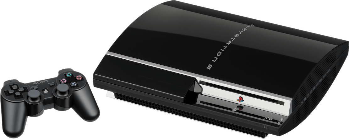
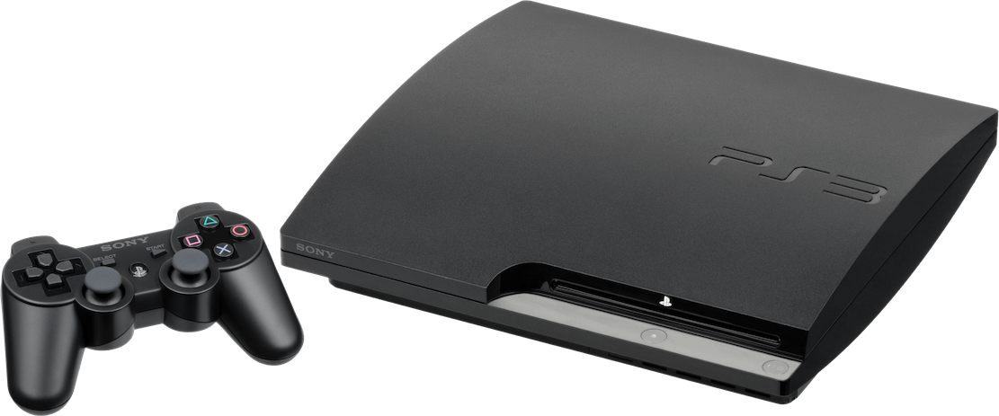
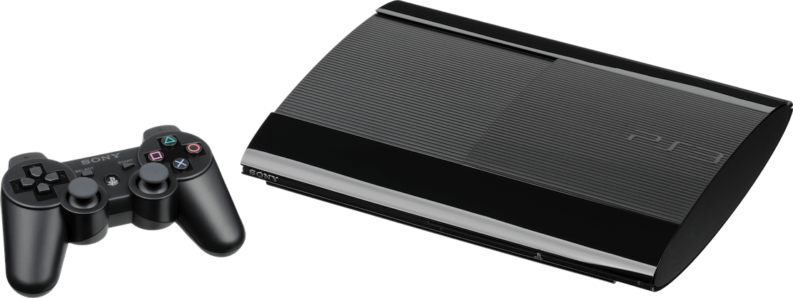
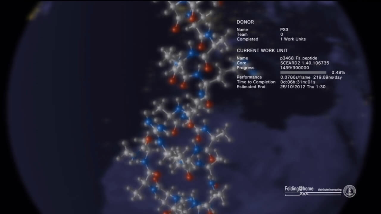
The original PlayStation 3 or 'PS3'. Released on 11/11/2006 in Japan, 17/11/2006 in America and 23/03/2007 in EuropeThe PS3 2000/3000 series (a.k.a. 'Slim'). Released on 01/09/2009 in Europe and America; and 03/09/2009 in JapanThe PS3 4000 series (a.k.a. 'Super Slim'). Released on 09/2012 internationally
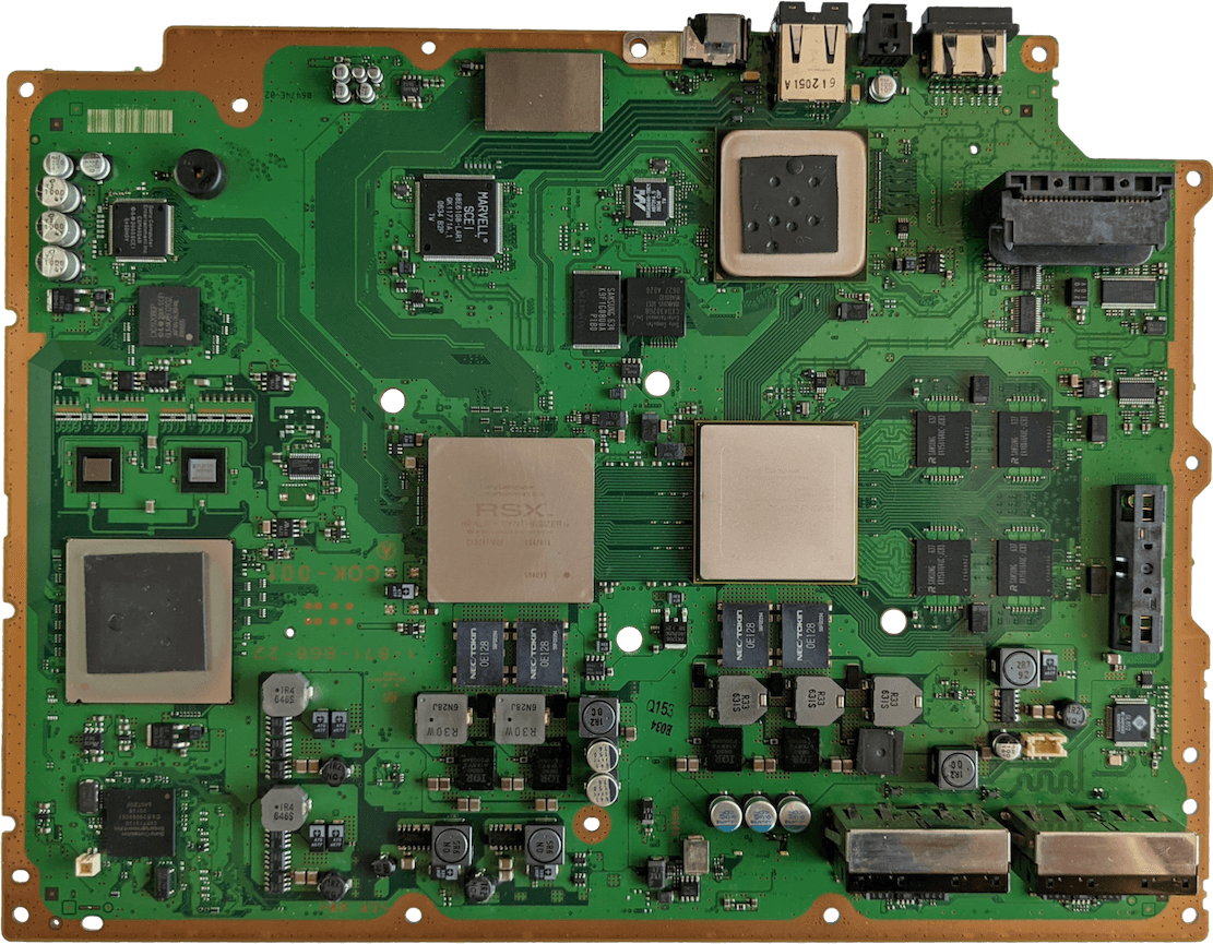
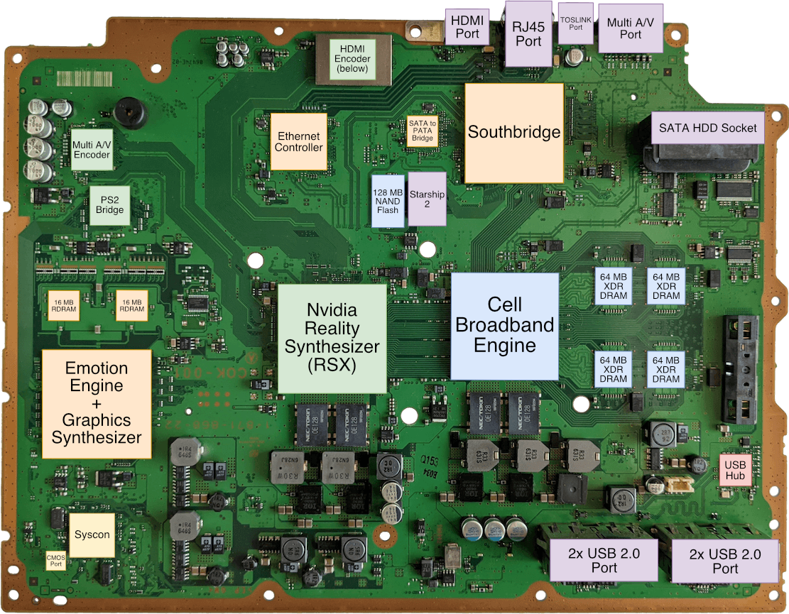
Motherboard Showing COK-001 revision (the first one), taken from my CECHA12 model. The remaining 128 MB NAND Flash and the connectors for the Blu-ray PATA drive, Wi-Fi/BT daughterboard, front panel and MultiCard reader are fitted on the backMotherboard with important parts labelled
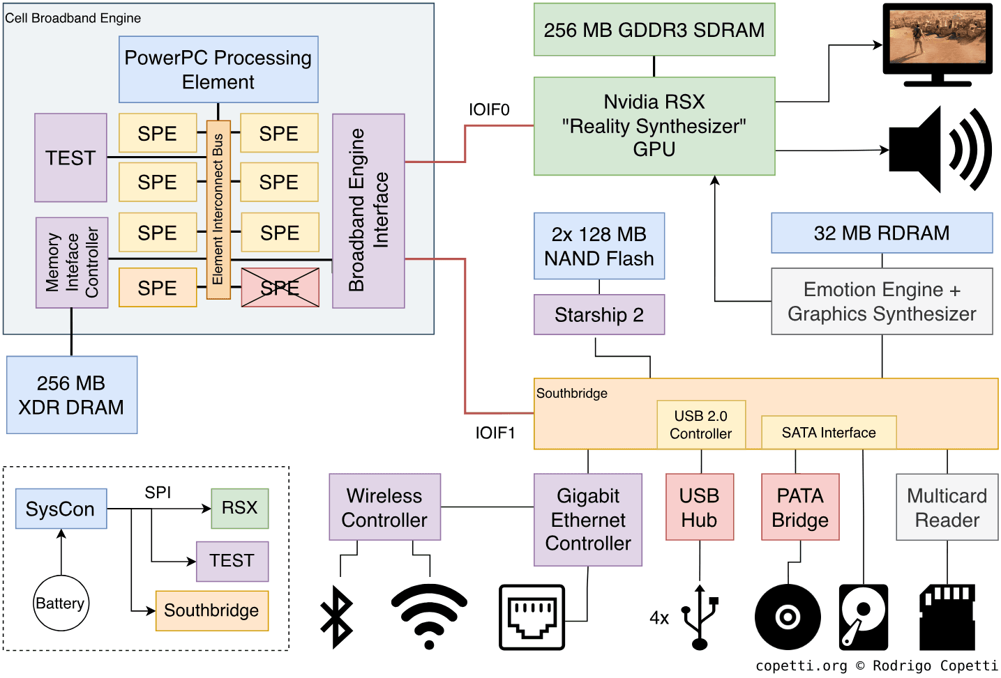
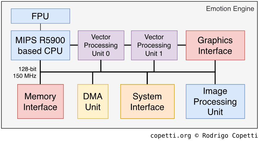
DiagramMain architecture diagram
A quick introduction
In 2006, Sony unveiled the long-awaited ‘next generation’ video game console, a shiny (albeit heavy) machine whose underlying hardware architecture continues the teachings of the Emotion Engine, that is, focus on vector processing to maximise performance, even at the cost of complexity. Meanwhile, their new ‘super processor’, the Cell Broadband Engine, is conceived during a crisis of innovation and will have to keep up as trends for multimedia services evolve.
This write-up takes a deep look at Sony, IBM, Toshiba and Nvidia’s joint project, along with its execution and effect on the industry.
On the article’s length
I’m afraid this article is not the typical ‘lunchtime’ one that I usually write for other consoles in this series. If you are interested in every area of the PlayStation 3, you are in for the whole journey! Having said that, this writing encompasses ~6 years of research and development carried out by countless engineers, so I don’t expect you to digest it all at once. Please take your time (and breaks if needed) and if at the end you are hungry for more, help yourself at the ‘Sources’ section!
CPU
Welcome to the most recognisable and innovative part of this console.
Introduction
The PS3’s CPU is massively complex, but it’s also a very fascinating work of engineering that intersects complex needs and unusual solutions, prominent in an era of change and experimentation. So, before we step into the internals of the PS3’s CPU, I wrote the following paragraphs to bring some historical context into the article. That way, we’ll be able to decompose the chip from top to bottom in a way that not only you will understand how this chip works, but also get the reasoning behind major design decisions.
The PS1’s CPU (1994). Designed by LSI and Sony, using MIPS’ technology.The PS2’s Emotion Engine (2001). Designed by Toshiba, with MIPS’ technology, again.
Almost ten years after the introduction of the original MIPS-powered PlayStation, we find ourselves in the early noughties, and things are not looking good for SGI/MIPS. Nintendo recently ditched them for a low-end PowerPC core with IBM as their new supplier while Microsoft, the newcomer in this market, chose Intel and their x86 empire.
Sony has a history of grabbing existing low-end designs (cheap MIPS cores) and moulding them to achieve acceptable 3D performance at a reduced cost, a process that involved other companies like LSI (for the PS1’s CPU) and Toshiba (for the PS2’s Emotion Engine). This methodology carried on until 2004 with the release of the PlayStation Portable. So, what new MIPS amalgamation were they going to build for the PlayStation 3?
Well, it turns out the development of the PlayStation 3 predates the PlayStation Portable one [1]. In 2000, months after the PS2’s release, Sony formed an alliance with IBM and Toshiba called ‘STI’ with the sole goal to deliver the next chip that could power the next generation of supercomputers [2]. If this didn’t sound extravagant enough, the next chip would also be used on the successor of the PS2. In the end, in 2004, IBM unveiled the Cell Broadband Engine (also known as ‘Cell BE’ or just ‘Cell’) [3].
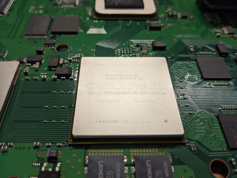
The Cell Broadband Engine chip. Unfortunately too shiny for my camera.
To understand Cell’s radical proposal, we must first take into account the problems affecting that era (late 90s-early 00s).
Every year, consumers ask for more speed. That’s always been the case. However, the last approach used to solve that (pipeline the datapath and step up the clock frequency) is now failing to scale. Intel’s NetBurst can’t evolve any further and its promised successor is nowhere to be seen. Similarly, IBM’s PowerPC 970/G5 can’t deliver its ‘3 GHz’ promise nor their low-power CPU (hence Apple can’t ship any laptop carrying their last-gen CPU) [4]. All in all, it looks like engineers have a new scalability crisis on their hands.
So, the focus turns to distributed computing[5]. In other words, why obsess with cranking up the performance of a single machine where you could instead have multiple smaller machines distributing their workload? Conversely, this approach is anything but new, considering all of the consoles analysed on this website contain more than one processor. However, it’s the development of a ‘single processor with multiple cores’ that opens up new opportunities for CPU design (which are not necessarily limited to the console market).
Consequently, Cell is part of this new wave of research and development. This new CPU combines a multi-core design with a special focus on vector processing. If you remember, vector computing is optimal for simulations (physics, lighting, etc) and it was previously materialised in the form of the Geometry Transformation Engine or the Vector Units, but you’ll soon see why Cell’s design is a huge step forward from the previous two.
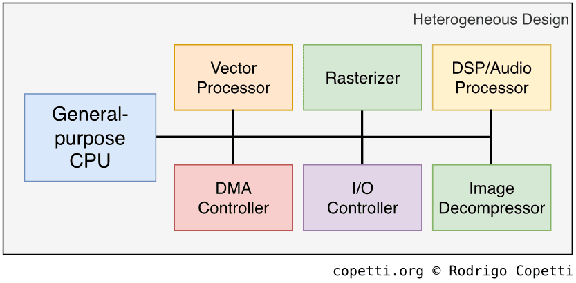
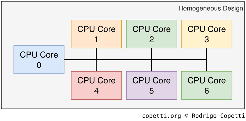
Example of heterogeneous design. This has been the de-facto architecture of many powerful consoles to this date.Example of homogeneous design. Each core can carry the same tasks as before, but they are not necessarily restricted to such task.
If you stop to think about it, both the PS1’s CPU and the Emotion Engine were already multi-core processors. So why was there so much fanfare about Cell? Well, the previous two chips were composed of one general-purpose core and several application-specific cores (i.e. audio processor, image decompression, etc) mixing different architectures, where the general-purpose core is in charge of commanding the others.
This type of CPU design is called Heterogeneous computing and it’s been the de-facto choice for building machines that are specialised in a particular set of applications (gaming, in this case). Its counterpart, Homogeneous computing, is more predominant on the PC market, where CPUs are required to perform a wider range of tasks (and they all have the same priority). Hence, the latter type may house multiple cores, but of the same type.
Back on topic, Cell combines both models: there are two types of cores in this CPU, one general-purpose ‘leader’ and eight vector ‘assistants’. These vector cores may take up various roles, and in doing so, they fulfil previous tasks that were originally solved by heterogeneous designs, but since Cell’s vectors are not limited to a single type of task, their cores provide the flexibility of homogeneous computers. All in all, this design is not perfect and will inherit some compromises, but throughout this writing, you’ll see the different problems that Cell will attempt to solve and how it managed to do so.
Having explained all that history and theory, I think we are ready to bring forward the protagonist of this section. This is Cell…
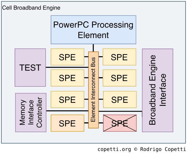
The Cell Broadband Engine (PS3 variant). Designed by IBM for supercomputing and scientific simulation. The crossed out ‘SPE’ means it’s disabled (unusable). The other ‘SPE’ on the left is reserved to the operating system.
… and by the end of this section, you’ll know what each component does.
Overall structure
Cell runs at a mighty3.2 GHz and it’s composed of a multitude of components. So, for the sake of this analysis, this CPU can be divided into three main areas [6]:
The leader: this is the part of Cell that directs the rest of the circuitry. Here we find a component called PowerPC Processing Element (PPE).
The assistants: these are as crucial as the PPE, but their capabilities are limited to an assistant/accelerator role. This group comprises eight Synergistic Processing Elements (SPEs).
The interfaces: As the need for bandwidth surges exponentially, newer interfaces are implemented to move data around without producing bottlenecks. In the interfaces group, we find a handful of protocols: the Element Interconnect Bus (EIB), the Broadband Engine Interface Unit (BEI), the Memory Interface Controller (MIC) and the Flex I/O buses.
This information will be revisited throughout the article in more depth, so you don’t have to memorise these names. The main goal of this section is to let the reader get a mental image of the nature of Cell and familiarise with all the components we’ll be discussing in due time.
How this study is organised
Seeing the previous structure, I had to organise this so you don’t get fed up with lots of information. Thus, we are going to analyse Cell by studying each component in this order:
The bus connecting all components, the Element Interconnect Bus (EIB).
The PowerPC Processing Element (PPE) and its core element, the PowerPC Processing Unit (PPU).
What general-purpose memory is available in this console.
The Synergistic Processing Elements (SPE) and their core element, the Synergistic Processing Unit (SPU).
The programming model devised to program Cell efficiently.
That being said, let’s begin the real analysis.
Inside Cell: The heart
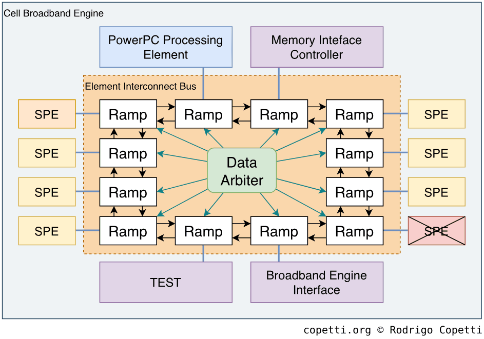
Since its announcement, Cell has been referred to as a Network-on-Chip (NoC) [7] instead of the traditional System-on-Chip (SoC) definition; this is attributed to Cell’s unorthodox data bus, the Element Interconnect Bus (EIB). We’ve seen so far how demanding CPU components can be, in addition to how susceptible a system is to bottlenecks. Well, to tackle this for the eleventh time, IBM has devised a new design… and has documented it using terms analogous to road driving.
Simplified diagram of the Element Interconnect Bus (EIB). Each arrow between ‘Ramps’ (nodes) represents two unidirectional buses, thus, each node is connected to the next one using four channels.
The EIB is made of twelve nodes called Ramps, each one connecting one component of Cell. Ramps are interconnected using four buses, two of them travel clockwise and the other two do so anti-clockwise. Each bus (or channel) is 128-bit wide. Having said that, instead of recurring to single bus topologies (like the Emotion Engine and its precursor did), ramps are inter-connected following the token ring topology, where data packets must cross through all neighbours until they reach the destination (there’s no direct path). Considering the EIB provides four channels, there’re four possible routes (rings).
Now, you may think, what’s the point of a token ring if data may end up travelling longer paths (compared to a single direct bus)? Well, a single bus is highly susceptible to congestion. Hence, EIB’s engineers decided on this topology to tackle large amounts of concurrent traffic (keep reading if you want to know how the token ring helped).
Data is transferred in the form of 128-bit packets[8]. Each ring can carry up to three concurrent transfers as long as the packets don’t overlap. The EIB operates with the use of command credits, in other words, whenever a component needs to initiate a transfer, it sends a request to the EIB’s Data Arbiter, which manages the traffic within the rings. The moment the request is approved, packets enter the ring and receive a ‘token’, which the data arbiter uses as meta-data to supervise the transfer. Moreover, some components have preferential priority over others, like the Memory Interface Controller (MIC) component, which is where main RAM is located. Finally, the data arbiter will never place packets at rings whose path is longer than half of the ring.
Each ramp plays a part in the transfer: they read the destination address of the packet to know whether to post data to their respective component or forward it to the next Ramp. During each clock cycle, ramps can receive and send 128-bit (16 Bytes) packets at the same time. So, considering there are four channels and the EIB operates at 1.6 GHz (half of Cell’s speed), the theoretical maximum transfer rate is 16 Bytes x 2 transfer/clock x 4 rings x 1.6 GHz = 204.8 GB/s. This value is of course too optimistic and there are many other external factors (i.e. origin/destination path, state of the bus, etc.) conditioning performance. In any case, many research papers made by IBM and other authors compiled more realistic speeds using practical experiments [9].
Now that you’ve seen how every component of Cell is interconnected, it’s time to check out the first component of this chip…
Inside Cell: The leader
Here we will take a look at the ‘main part’ of Cell. That is the part of the silicon that is in charge of commanding the rest. The component’s name is PowerPC Processing Element (PPE) and you can think of it as the MIPS R5900 of the Emotion Engine.
Composition of the PPE
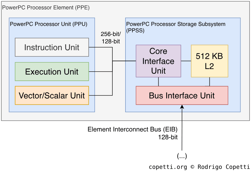
Remember how I divided Cell into different areas before? Well, the same can be done with the PPE. IBM uses the term ‘element’ to describe the independent machine [10], but once inside it uses the term ‘unit’ to separate the core circuitry from the interfaces that communicate with the rest of Cell.
Simplified diagram of the PowerPC Processing Element (PPE).
Having said that, the PowerPC Processor Element is surprisingly composed of two parts:
PowerPC Processing Unit (PPU): This is the logical part of the PPE (the ‘core’). Don’t forget this is not Nintendo’s PPU! (even though they are sharing the same letters of the Latin alphabet… in the same order…).
PowerPC Processor Storage Subsystem (PPSS): The big interface that connects the PPU to the outside world. Furthermore, it provides a whopping 512 KB of L2 cache.
As you can see, the design of the PPE (and the rest of Cell) is pretty modular, which follows the teachings of RISC design, you’ll soon see that the modularity is applied even inside the PPU.
The PowerPC Processing Unit
We are going to take a look at the insides of the PPU just now. To recap, we’ve dived into Cell, then into the PPE, and finally into the PPU. We’ll analyse the PPU just like any other CPU core.
To start with, the PPU is not built from the ground up but re-purposes existing PowerPC technology. However, unlike previous iterations where IBM grabbed an existing processor and half-updated it to meet new requirements, the PPE doesn’t replicate any previous CPU design. Instead, IBM constructed a new CPU that follows version 2.02 of the PowerPC specification (which happens to be the last PowerPC spec before being rebranded to ‘Power ISA’). To sum up, you won’t find the PPU’s design on any existing chip from that time, yet, it’s programmed using the same machine code as other PowerPC chips.
That being said, why did IBM choose PowerPC technology to develop a high-performance chip? Simple, PowerPC is a mature platform [11] that enjoyed ~10 years of Macintosh user-base testing and revisioning, it ticks all the boxes in Sony’s list and, if the need arises, it can be adapted to different environments. Last but not least, the use of a well-known architecture is good news for existing compilers and codebases which, for a new console, is a big starting advantage.
It’s worth mentioning that IBM was one of the authors of the first PowerPC chips, along with Motorola and Apple (recall the AIM alliance). Be as it may, towards the early 00s, the so-called alliance members were already working separately, where Motorola/Freescale developed a different PowerPC series from IBM.
The PPU shares some history with the PowerPC 970 (called G5 by Apple), both are descendants of POWER4, a PowerPC predecessor mainly used in workstations and supercomputers. This will become more evident when I show you the modularised execution units soon. This is a radical change compared to the GameCube’s 750-line CPU, which had considerable input from Motorola but was then slightly modified by IBM.
Back on topic, the PPU is a complete 64-bit processor. This means:
The size of a word is 64-bits.
There are 64-bit general-purpose registers (32 to be exact).
The data-bus is at least 64-bit wide: in the next sections of the article, you’ll see it’s much wider than that, but for now, keep in mind that transferring 64-bit words won’t penalise performance.
The address bus is 64-bit wide: in theory, the CPU can access up to 16 exabytes of memory. Now, in practice, this is very costly if the machine doesn’t house all that memory. So, modern CPUs delegate addressing to the Memory Management Unit (MMU) to provide more uses to the address bus.
Finally, the PPU implements the PowerPC ISA version 2.02, including optional opcodes for floating-point square root [12]. It’s also been extended with a group of SIMD instructions called Vector/SIMD Multimedia Extension (VMX). On the other side, some elements are missing from the original specification, such little-endian mode (in fact, Cell only operates in big-endian) and just a handful of opcodes.
By applying a ‘microscopic’ view to the PPU, we can observe this unit is composed of different blocks or sub-units which perform independent operations (load values from memory, carry out arithmetic, etc). The capabilities of the PPU are defined by what each block can do and how:
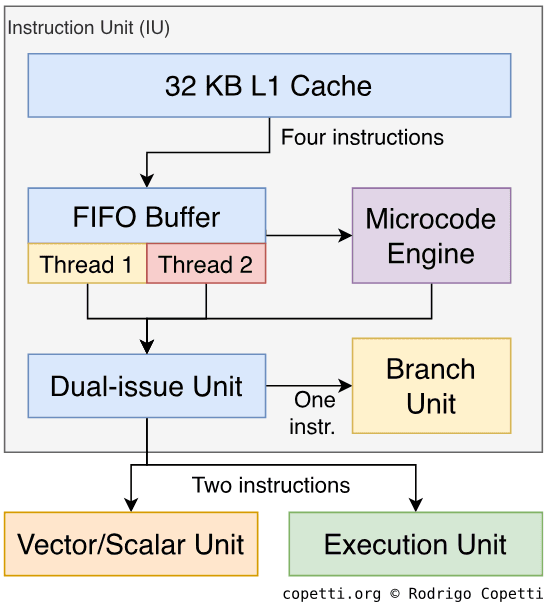
The first block is called Instruction Unit (IU) and as its name suggests, it pulls instructions from L2 cache and signals other units to perform the requested operation. Like its i686 contemporaries, part of the instruction set is interpreted with the use of microcode (the IU embeds a small ROM for this purpose). Lastly, the IU also houses 32 KB of L1 cache for instructions.
Instruction issuing is carried out with a 12-stage pipeline, though in practice the total number of stages will greatly vary depending on the type of instruction. For instance, the branch prediction block may bypass great parts. If we combine the IU with the neighbour units, the final number of stages is often close to 24 (yes, it’s a big number, but remember Cell runs at 3.2 GHz).
Now for the interesting parts, The IU is dual-issued: in some cases, the IU will dispatch up to two instructions at the same time, consequently improving throughput greatly. In practice, however, there are many conditions for this to work, so programmers/compilers are responsible for optimising their routines so their sequence of instructions can take advantage of this function. By the way, dual-issuing has been implemented by previous CPUs as well, and the term varies between vendors, so here I used IBM’s definition.
Furthermore, to top it off, the IU is also multi-threaded, where the unit can execute two different sequences of instructions (called ‘threads’) at the same time. Behind the scenes, the IU is just alternating between the two threads at each cycle, giving the appearance of multi-threading. This technique is historically known as Simultaneous Multi-Threading (SMT) or hyper-threading, as Intel later coined. Nevertheless, IBM’s multi-threading mitigates unwanted effects like pipeline stalls, since the CPU will no longer be blocked if one instruction jams up the flow. To accomplish multi-threading, IBM engineers duplicated the internal resources of the IU, which includes general-purpose registers (previously I said there are 32 registers available, that’s per thread. In reality, there are 64 in total!), however, resources that don’t belong to the PowerPC specification (such as L1 and L2 cache; and the interfaces) are still shared. Thus, the latter group is single-threaded.
All in all, combining dual-threading with dual-issuing, the PPU can execute up to four instructions per cycle. Even though this is a ‘best-case scenario’, it still provides optimisation opportunities that users will ultimately notice in the game’s frame rate!
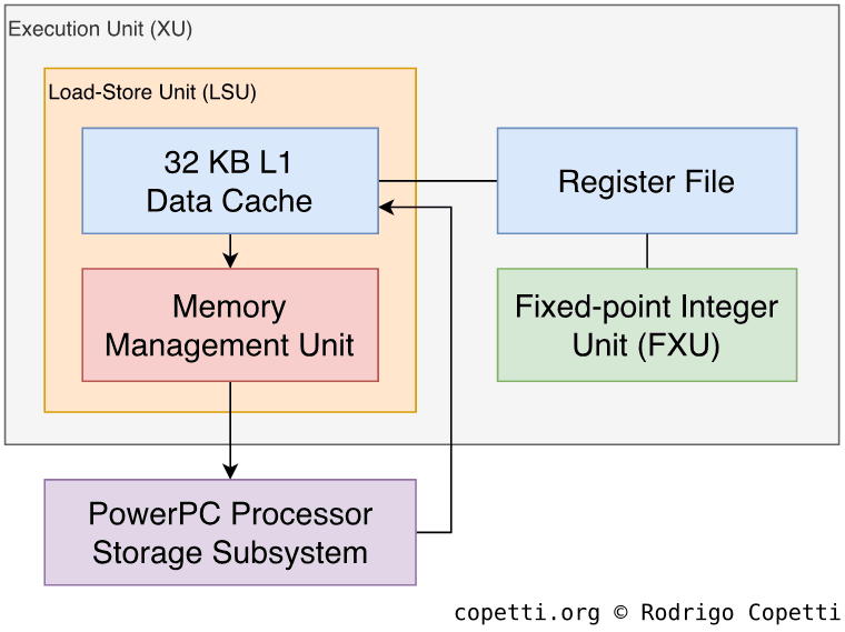
Simplified diagram of the Load-Store Unit (LSU) and its neighbours.
The following blocks grant the PPU the ability to execute load-store instructions and carry out memory management.
To begin with, the Load and Store Unit (LSU) executes ‘load’ and ‘store’ opcodes backed by 32 KB of L1 data cache. As a consequence, this unit has direct access to memory and the register file.
Furthermore, the LSU is coupled with a Memory Management Unit (MMU), which is a common occurrence in contemporary hardware. To make a long story short, the MMU handles memory addressing using a virtual address map combined with memory protection. To improve the latter, this MMU in particular features a segment unit, which groups memory addresses using ranges called ‘segments’. Now, to prevent performance degradation in the process, a Translation Lookaside Buffer (TLB) (caches converted addresses) and a Segment Lookaside Buffer (SLB) (caches segments) are included.
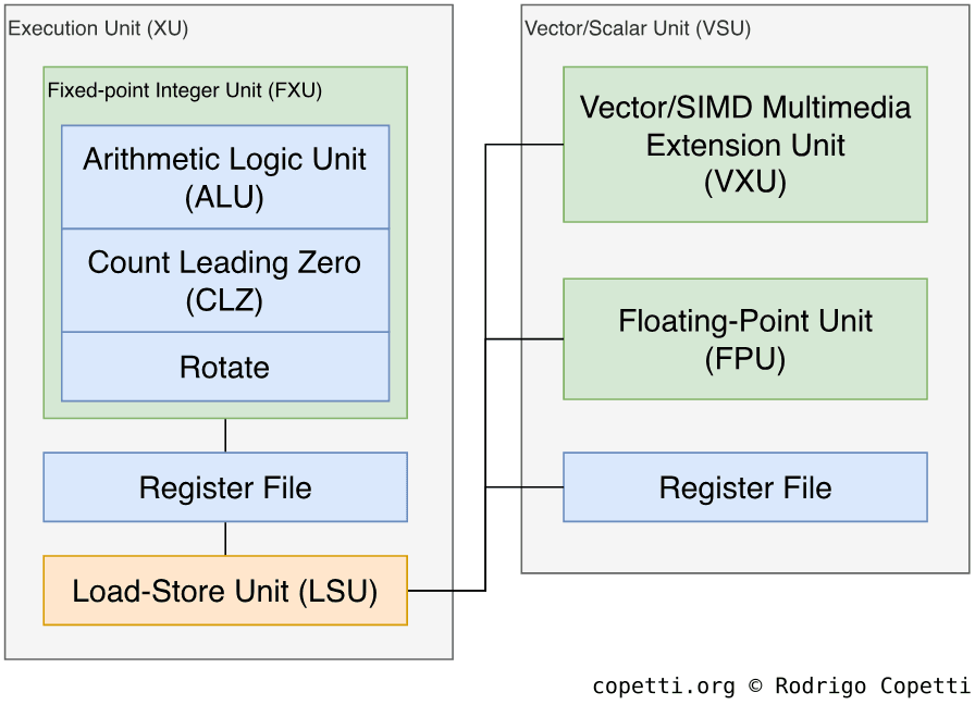
Simplified diagram of the units that perform arithmetic.
There are only two more units of the PPU left to explain: the ones computing the math any game will need.
The first one is a traditional Fixed-Point Integer Unit (FXU). It carries out integer arithmetic, such as division, multiplication, bit rotation (similar to bit shifting but discarded bits are returned to the other end) and count-leading zero (useful for normalising vertex coordinates, for instance). Its pipeline is 11 stages long.
If you look at the diagram, you’ll see that the FXU, LSU and MMU are grouped into a single unit called Execution Unit (XU), this is because they share the same register file.
The second unit is way more interesting, the Vector/Scalar Unit (VSU) performs operations with floating-point numbers and vectors. It’s made up of a 64-bit FPU (follows the IEEE 754 standard) and a Vector/SIMD Multimedia Extension unit (VXU), which executes a set of SIMD instructions called VMX. The latter operates 128-bit vectors made from sixteen 8-bit values to four 32-bit ones [13]. You may have heard about this extension before, as ‘VMX’ is IBM’s name to Motorola’s ‘AltiVec’ or Apple’s ‘Velocity Engine’ (long live trademarks). Conversely, Cell’s competitive SIMD capabilities are found in another processor, so don’t relax just yet!
You’ve just seen how the PPE works and what it’s made of, but what does it mean for a developer?
After all, the PowerPC Processing Element is only a general-purpose processor, but here’s the thing: it’s not meant to work alone. Remember that wide main bus (the EIB)? IBM designed the PPE so engineers may combine it with other processors to accelerate particular applications (i.e. HPC, 3D graphics, security, scientific simulations, networking, video processing, etc) and since this writing is about the PlayStation 3, you’ll see the rest of Cell is treated with computer graphics and physics in mind, so, the rest of the article reflects that purpose.
Outside Cell: Main Memory
Let’s now step out of Cell for a moment, as it doesn’t matter how good the PPE is if we don’t have a proper working space (memory) to put it to work.
Thus, Sony fitted 256 MB of XDR DRAM on the motherboard… But, again, what does this mean? To answer that, we need to take a look at how the memory blocks work and how they connect to Cell.
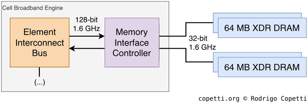
Cell next to the four 64 MB XDR DRAM chips.
First of all, the type of memory fitted is called Extreme Data Rate (XDR). You may recognise XDR DRAM as the successor of the jinxedRDRAM found in the Nintendo 64 and the PlayStation 2. But don’t jump to conclusions just yet!
Rambus, like any other company, improves upon their inventions. Their third revision (XDR) now operates at octa-rate (four times the rate of its adversary, DDR DRAM) [14]. Latency doesn’t pose an issue anymore, if we take a look at one of its manufacturers’ data-sheets, XDR’s latency is reported between 28 ns and 36 ns [15], almost 10 times faster than the first-generation RDRAM chips.
The first revision of the PlayStation 3’s motherboard contains four 64 MB chips, handled in pairs. XDR is connected to Cell using two 32-bit buses, one on each pair. So, whenever the PPU writes a word (64-bit data), it’s split between two XDR chips. The latter are clocked at 400 MHz [16].
Cell’s memory architecture diagram.
Cell connects to the XDR chips using the Memory Interface Controller (MIC), another component within Cell (like the PPE). Additionally, the MIC buffers memory transfers to improve bandwidth, but it has a big limitation: large byte alignment. In essence, the MIC’s smallest data size for transfers is 128 Bytes, which works well for sequential reads or writes. But if the data is smaller than 128 B or it requires alternating between writing and reading, performance penalties appear.
That being said, is the MIC a bottleneck or an accelerator? Well, you have to put it into perspective, bandwidth optimisation is critical in data-hungry systems. In the past, we’ve seen solutions like the write-gather pipe or the write back buffer, so the MIC is simply a new proposal to a recurring problem. For what it’s worth, Sony claims the transfer rate is 25.6 GB/s. Still, there are too many factors that will condition the final rate in practice (you’ve seen how convoluted it is to move data from one place to another within Cell).
This is as far as it goes for main RAM, but there’s more memory elsewhere: the hard drive. The PS3 also enables games to use 2 GB from its internal hard drive as a working area (similarly to what the original Xbox provided) [17].
Inside Cell: The assistants
We’ve seen before how Sony always supplies a general-purpose processor (the PPE in this case) accompanied by accelerators to reach acceptable gaming performance (the VPUs and IPU in the case of the PS2; and the GTE and MDEC with the PS1). This is common practice with video game console hardware, as general-purpose units can perform a wide range of tasks, but are not specialised in anything. Game consoles require only a subset of skills (physics, graphics and audio, for instance) so co-processors bring them up to their task.
[The PPE] is a watered-down version to reduce power consumption. So it doesn’t have the horsepower that you see in say a Pentium 4 (…) If you take the code that runs today on your Intel or AMD, whatever your power, and you recompile it on Cell, it’ll run today - maybe you have to change the library or two, but it’ll run today here, no problem. But it’ll be about 60% slower, 50% slower and so people say “Oh my god! This cell processor’s terrible!” but that’s because you’re only using that one piece[18].
– Dr. Michael Perrone, manager of the IBM TJ Watson Research Center’s Cell Solutions Department
The accelerators included within PS3’s Cell are the Synergistic Processor Elements (SPE). Cell includes eight of them, although one is disabled while the console boots up. This is because chip fabrication requires an exceptional amount of precision (Cell initially used the 90nm fabrication process) and the machinery is not perfect. So, instead of chucking out circuitry that came out < 10% defective, Cell includes one spare SPE. Thus, if one of them comes out defective, the whole chip is not discarded. Now, that spare SPE will always be deactivated, regardless of whether it’s working or not (Sony can’t have two different PS3s in the market).
Composition of the SPE
Moving on, the Synergistic Processor Element (SPE) is a tiny independent computer inside Cell and commanded by the PPE. Remember what I explained before about the adoption of elements from homogeneous computing? Well, these coprocessors are somewhat general-purpose and not restricted to a single application, so they will be able to assist in a wide range of tasks, that is, as long as developers can program them properly.
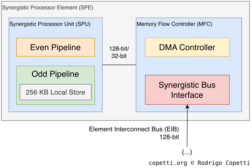
Simplified diagram of the Synergistic Processor Element (SPE), there are eight of these within Cell (one disabled).
Just like we did with the PPE, we’ll have a look at the SPE. It’s a shorter one so if at the end, you’d like to learn more about the SPEs, check out the ‘Sources’ section at the end of the article. That being said, let’s start…
The SPE is a processor that follows similar structuring to the PPE, being made of two parts:
The Memory Flow Controller (MFC) is the block that interconnects the core with the rest of Cell, this is equivalent to the PowerPC Processor Storage Subsystem (PPSS) in the PPE. The MFC’s main job is to move data between SPU’s local memory and Cell’s main memory and keep the SPU in sync with its neighbours.
To perform its duties, the MFC embeds a DMA controller to handle communication between the EIB and the SPU’s local memory. Furthermore, the MFC houses another component called Synergistic Bus Interface (SBI) that sits between the EIB bus and the DMA controller. It’s a very complex piece of circuitry to summarise, but it basically interprets commands and data received from outside and signals the internal units of the SPE. As the front door to Cell, the SBI operates in two modes: bus master (where the SPE is adapted to request data from outside) or bus slave (where the SPE is set to receive orders from outside).
As a curious fact, considering the limit of EIB packets (up to 128-bit long), the MFC’s Direct Memory Access block can only move up to 16 KB of data per cycle, otherwise, the EIB throws a ‘Bus Error’ exception during execution [19].
The Synergistic Processor Unit (SPU) is the part of the SPE where the core processor resides, equivalent to the ‘PPU’ when we talked about the PPE.
Contrariwise to the PPU, the SPU is isolated from the rest of the Cell. Thus, there’s no shared memory between the PPU and others SPUs. Instead, the SPU contains local memory used as working space. However, the contents of local memory can be moved back and forth using the MFC.
In terms of functionality, the SPU is a lot more limited than the PPU. For instance, SPU doesn’t include any memory management functions (address translation and memory protection) or even state-of-the-art functions (i.e. dynamic branch prediction). Nonetheless, it performs exceptionally well at vector processing.
To program this unit, developers use the PPU to invoke routines provided by the PlayStation 3’s Operating System, these upload the executable specifically written for the SPU to the SPU of choice and signal it to start execution. Afterwards, the PPU keeps a reference of the SPU’s thread for synchronisation purposes [20].
Like any CPU, the Synergistic Processor Unit (SPU) is programmed using an instruction set architecture (ISA). Both SPU and PPU follow the RISC methodology, however, unlike the PPU (which implements a PowerPC ISA), the SPU’s ISA is proprietary and mainly composed of a SIMD-type instruction set. As a result, the SPU features 128 128-bit general-purpose registers which house vectors made of 32/16-bit fixed-point or floating-point values. On the other side, to preserve memory, SPU instructions are much smaller, just 32 bits long. The first part contains the opcode and the rest can reference up to three operands to be computed in parallel.
This is very relatable to the previous Vector Floating Point Unit debuted in the PS2, but a lot has changed since then. For instance, the SPU doesn’t require developers to learn a new proprietary assembly language - IBM and Sony provided toolkits to program the SPUs using either C++, C or assembly.
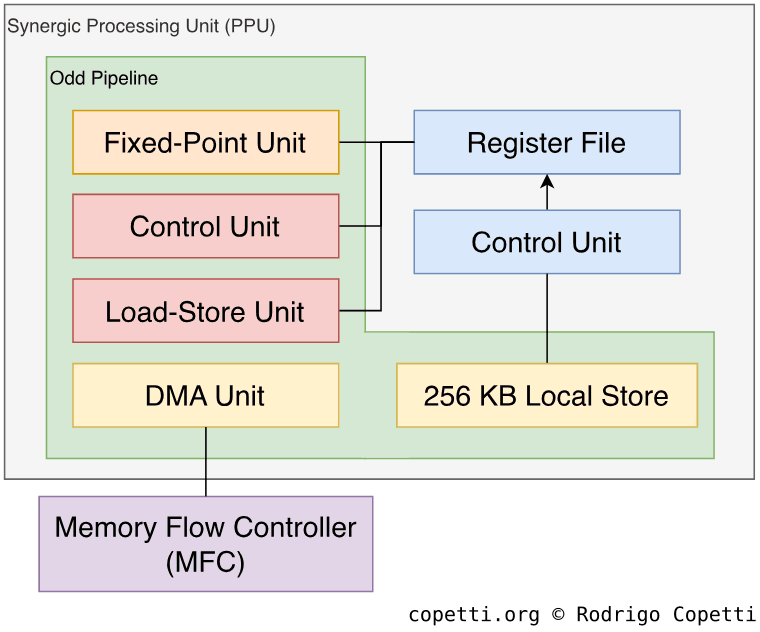
In terms of design, this processor doesn’t execute all instructions using the same unit, execution is instead divided into two blocks or ‘execution pipelines’, one is called Odd Pipeline and the other is named Even Pipeline. These two pipelines execute different types of instructions, enabling the SPU to issue two instructions per cycle whenever it’s possible to do so. On the other hand, the SPU will never dual-issue instructions that depend on each other, thus, mitigating data hazards that may emerge.
The Odd pipeline executes most of the instructions except the arithmetic ones.
First of all, you’ll find the SPU Load/Store unit (SLS) does three essential things:
Houses 256 KB of local memory to store instructions and data. The type of memory fitted is single-ported (considering this is a critical area, it’s a bit disappointing they didn’t use dual-ported chips…). Furthermore, the address bus is 32-bit long.
Executes load and store instructions.
Forwards instructions to another block for issuing.
Notice that there are only 256 KB available to store the program. Considering SPU programs can be compiled using C/C++, it’s not easy to predict how large the binary will be. For this reason, it is recommended that developers assume there is only half the memory available (128 KB) [22], which leaves enough window for the compiled code to take up as much space as it needs, although this comes at the cost of storage and efficiency.
Finally, there’s also a SPU Channel and DMA Transport (SSC) unit, which the Memory Flow controller uses to fill and/or fetch local memory, and a punyFixed-Point Unit that only does shuffling and vector rotation.
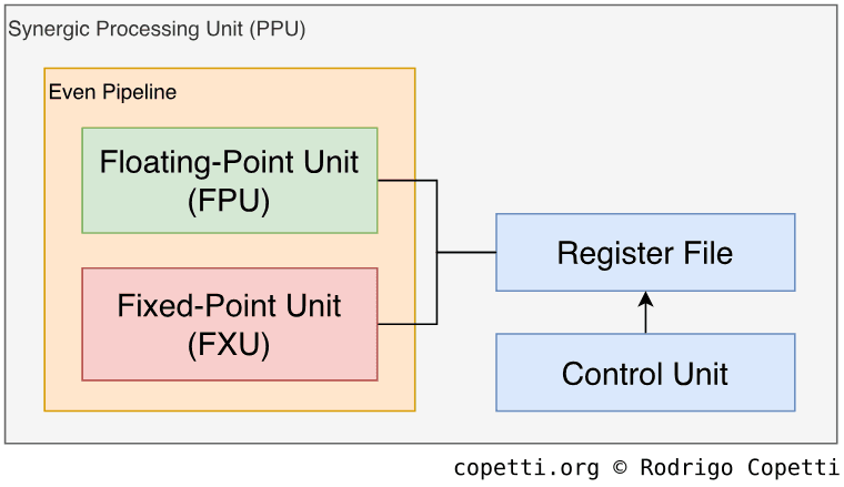
The Even pipeline is notable for its arithmetic capabilities.
In here we find a realFixed-point Unit (FXU) which performs basic arithmetic, logical operations (AND, OR, etc), and word shifts.
Last but not least, we’ve got a Floating-point Unit (FPU) which performs single-precision (32-bit float), double-precision (64-bit double) and integer (32-bit int) operations. It follows IEEE standard with some deviations (floats behave similarly to the PS2).
As we reach the end of Cell, you may ask how are developers supposed to program this monster? Well, similarly to the previous programming models devised for the Emotion Engine, IBM proposed the following methodologies [23]:
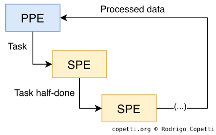
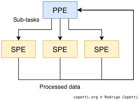
Representation of the multistage pattern, where the PPE assigns a task that gets passed around each SPE, and eventually returned with the data processed.Representation of the parallel pattern, where the PPE assigns a subtask to each SPE, and in turn each SPE returns the processed data, which the PPE merges.Representation of the services pattern, where the PPE allocates a different task to each SPE, and each work individually to fulfil it.
PPE-centric approaches are a set of programming patterns that place the main responsibilities on the PPE and leave the SPE for offloading work. There are three possible patterns:
Multistage pipeline model: the PPE is tasked with sending work to a single SPE, which in turn performs the required computations and passes the results to the next SPE. This continues until the last SPE in the chain sends the processed data back to the PPE.
For obvious reasons, IBM doesn’t suggest this design for primary tasks as it requires a considerable amount of bandwidth and it tends to be difficult to maintain.
Parallel stages model: the PPE divides its main task into independent sub-tasks and sends each one to a different SPE. Each SPE then returns the processed data to the PPE after they finish, then, the PPE combines it to produce the final result.
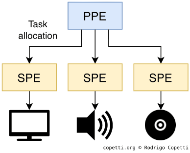
Services model: each SPE gets assigned a single job (i.e. MPEG decoding, audio streaming, perspective projection, vertex lighting, etc) and the PPE is in charge of sending raw data to the designated SPE. While waiting, the PPE carries out other functions.
While this implies each SPE will have a single job, their job designation is not meant to last forever. The PPE must reallocate different jobs on the fly as the needs of the program change.
SPE-centric approaches
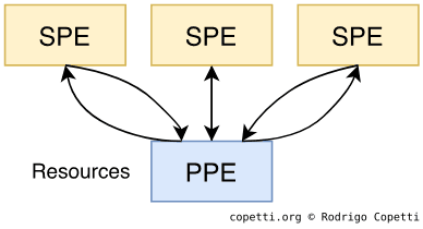
Representation of the SPE-centric pattern, where each SPE is in charge of its functionality and only interacts with the PPE to obtain a resource.
Instead of using the SPEs to serve the PPE, it’s the other way around. Using the internal DMA unit, SPEs fetch and execute tasks stored in main memory, while the PPE is limited to resource management.
This model is a lot more radical than the rest, in the sense that previous patterns are closer to the traditional and PC-like ‘general-purpose processor with co-processors’ paradigm. Thus, codebases implementing SPE-centric algorithms may be harder to port to other platforms.
Conclusion
As you can imagine, while the multi-core design of Cell accelerates emerging techniques such as procedural generation, none of these designs are particularly simple to implement, especially considering game studios prefer codebases that can be shared across different platforms.
To give you an example, the developers of the Unreal Engine 3 (Epic Games) demonstrated the limitations of the SPUs while trying to implement their collision detection system [24]. Their design relies on Binary Space Partitioning (BSP), an algorithm strongly dependent on comparisons (branching). Because the SPUs don’t provide dynamic branch prediction like the PPU, their implementation disappointed PlayStation 3 users when compared side-by-side against other platforms (i.e. Xbox 360 or i686 PCs, both of which provide consistent prediction techniques across all their cores). Hence, Epic Games had to resort to further optimisations only compatible with Cell.
I suppose it’s just a matter of time, patience and a lot of learning for software engineers to crank up the full potential of Cell. However, history demonstrated that’s not feasible for every studio, which makes me wonder if that’s the reason current console hardware (as of 2021) has homogenised so much.
Graphics
If you thought that Cell, with all its quirks, could take care of every task of this console, then let me tell you something hysterical: Sony fitted a separate chip for 3D graphics.
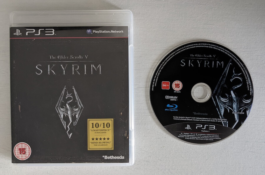
Uncharted 3: Drake’s Deception (2011).The Elder Scrolls V: Skyrim (2011).Killzone 3 (2011).One Piece: Pirate Warriors (2012).Example of PS3 games. All rendered at their maximum resolution (1280x720 pixels).
It appears that even with a supercomputer chip, Sony still had to fetch a GPU to finalise the PlayStation 3. This makes you wonder if IBM/Sony/Toshiba hit a wall while trying to scale Cell further, so Sony had no option but to get help from a graphics company.
We had started this ICE [Initiative For A Common Engine] team with the intent of developing some core technology that could be shared amongst all the first parties (…) For a while, [PS3 had] no GPU, it was going to run everything with SPUs. The ICE team proved to Japan that it was just impossible. It would be ridiculous. Performance-wise, it would be a disaster. That’s why they finally added the GPU, closer to the end [25].
– Unnamed sources from Naughty Dog
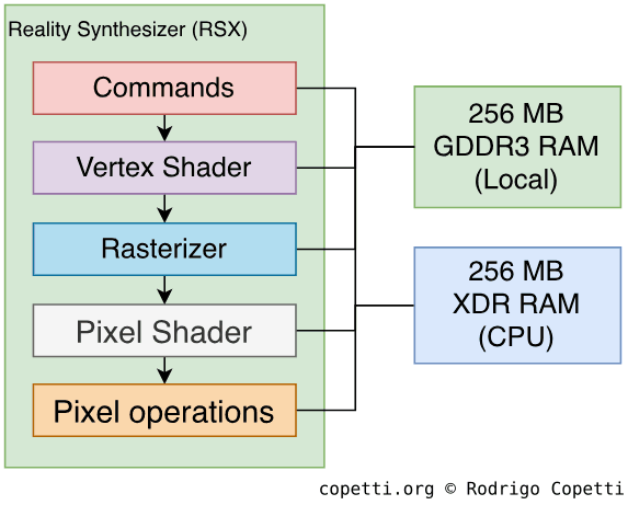
What I am sure is that the PS3 contains a GPU chip manufactured by Nvidia meant to offload part of the graphics pipeline. The chip is called Reality Synthesizer or ‘RSX’ and runs at 500 MHz[26]. Its clock speed looks concerning when compared to Cell’s (3.2 GHz), though you’ll soon see that the GPU is better equipped for computing huge amounts of operations in parallel. So it’s a matter of finding a balance between Cell and RSX when it comes to building the graphics pipeline (though I must confess this sounds simpler on paper than it is in practice).
I will now perform the same level of analysis previously done with Cell, this time focusing on RSX and its graphics capabilities.
Overview
It’s been five years since Nvidia debuted the GeForce3/NV30 lineup in 2001, and by then the arena was battled by strong players like 3dfx, S3 and ArtX/ATI. Though in subsequent years, the number of companies slowly reduced to the point that by 2006, only ATI and Nvidia remained as the flagship video card suppliers in the PC market.
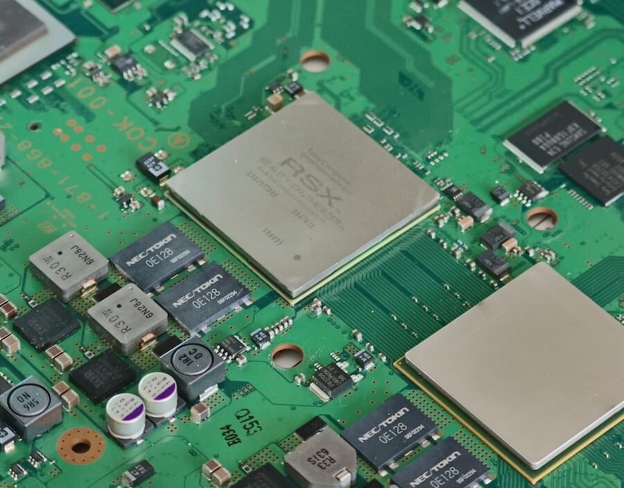
RSX chip next to Cell.
The RSX inherits existing Nvidia technology, it’s reported to be based on the 7800 GTX model sold for PCs, which implements the GeForce7 (or NV47) architecture [27], also named ‘Curie’.
In my previous Xbox analysis, I talked about the GeForce3 and their debuting pixel shaders, so what has changed since then? There have some been ups and downs, but mostly incremental changes, so nothing too groundbreaking compared to GeForce3’s pixel shaders.
On the other side, while the 7800 GTX relies on the PCI Express protocol to communicate with the CPU, the RSX has been remodelled to work with a proprietary protocol called Flex I/O[28], a distinct interface within Cell designed to connect to neighbouring chips. Flex I/O operates in two modes:
BIC mode for connecting other Cell processors (to be used in multi-processor environments).
The slower IOIF mode for connecting up to two peripherals, a ‘fast’ one and a ‘slow’ one.
Alas, the RSX is not Cell, so it goes through the IOIF protocol, using the fastest slot.
For comparison purposes, IOIF behaves as a 32-bit parallel bus with a theoretical bandwidth of up to 20 GB/s, while the PCI-express used in the 7800 GTX (x16 1.0) is a 16-bit serial bus with a theoretical bandwidth of up to 4 GB/s.
Organising the content
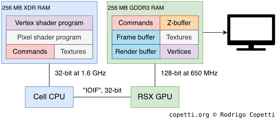
RSX has 256 MB of dedicated GDDR3 SDRAM at its disposal. Surprisingly, it’s the same memory type found in the Wii. The memory bus runs at 650 MHz with a theoretical bandwidth of up to 20.8 GB/s.
Example of how data is organised across the memory available. Notice how RSX can access its content from different memory chips.
Inside those 256 MB, Cell can place everything that RSX will need to render a frame. That includes vertex data, shaders, textures and commands. Now, thanks to Cell’s Flex I/O bus, RSX can also utilise the aforementioned 256 MB of XDR memory (CPU’s main RAM) as working space, though this will come with some performance penalties. This comes in handy if the rendered frame will be post-processed by an SPU, for instance.
As you can see, while this console didn’t implement a UMA architecture, it can still distribute graphics data across different memory chips if programmers decide to do so. I mention this because I wish many ‘technical explainers’ would read more about this feature before shouting over-summarising statements like “The PS3 was limited because it didn’t have UMA”. That may be true in certain cases, but unless they mention these, that generic claim is, in my opinion, misguiding.
Finally, RSX supports many forms of data optimisation to save bandwidth, examples include 4:1 colour compression, z-compression and ‘tiled’ mode (I’ll explain more about it later on).
Constructing the frame
Let’s now take a look at how RSX processes and renders 3D scenes.
Pipeline overview of the RSX.
Its pipeline model is very similar to the GeForce3, but super-charged with five years of technological progress. So I suggest checking out that article beforehand since this one will focus on the new features, I also recommend reading about the PlayStation Portable’s GPU because a lot of new developments and needs overlap with that chip. That being said, let’s see what we’ve got here… [29]
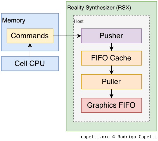
As with any other GPU, there must be a block of circuitry in charge of receiving the orders from outside. With RSX, this is handled by two blocks, Host and Graphics Front End.
The Host is responsible for reading commands from memory (either at local or main) and translating them into internal signals that other components in RSX understand, this is done with the use of four sub-blocks:
Pusher: fetches graphics commands from memory and interprets branch instructions. It also contains 1 KB of prefetch buffer. The processed commands are sent to the FIFO Cache.
FIFO Cache: stores up to 512 commands decoded by the Pusher in a FIFO manner to provide quick access.
Puller: as the name indicates, it pulls commands from the FIFO cache whenever RSX is ready to render and sends them to the next unit.
Graphics FIFO: stores up to eight commands that will be read by the Graphics Front End.
The Graphics Front end then reads from the Graphics FIFO and signals the required units inside RSX to compute the operations. If you remember, this is equivalent to the ‘pfifo’ in the GeForce3.
As you can see, commands and data pass through many buffers and caches before reaching the final destination. This is intentional, as it prevents stalling the pipeline due to different units and buses operating at different speeds. So, cached memory takes advantage of fast bandwidth whenever it’s possible.
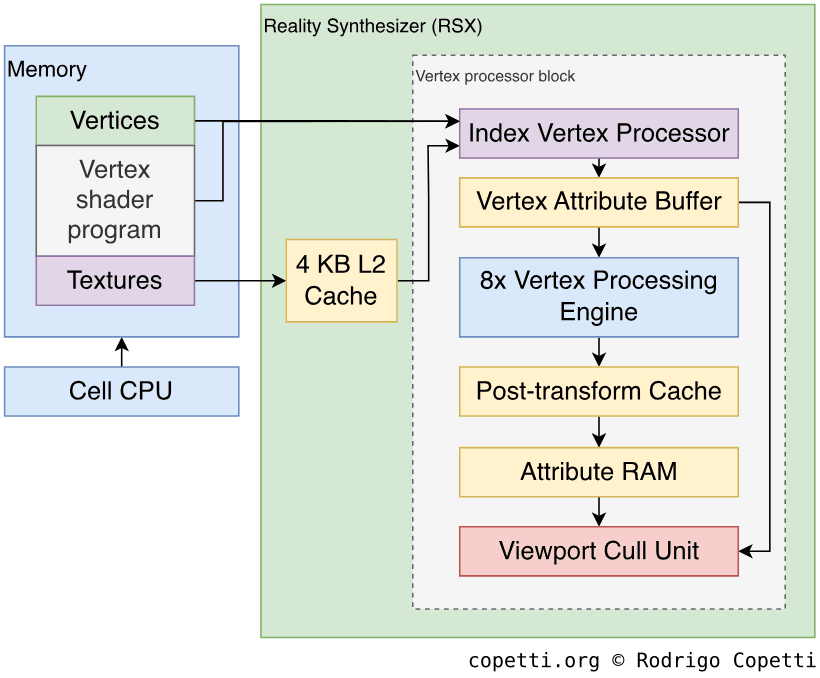
Diagram of the vertex stage process, notice that the Vertex Processing Engines (VPE) are bypassed if the vertices don’t need further processing by the vertex shader.
The next unit is the Geometry Processing block, an evolution of the ‘Vertex Block’ in the GeForce3 that performs vertex transformation. It’s still programmable with the use of vertex shaders, which is now a widely adopted feature in the graphics industry. Furthermore, the instruction limit has been increased to 512 instructions minimum (originally, 136 was the limit!).
The block that executes shaders is called Vertex Processing Engine (VPE) and it can process one vertex per clock cycle. As if wasn’t enough, there are eight VPEs working in parallel. Since the GeForce6 series, Nvidia has aligned its shader programming interface to a model called ‘Vertex Shader Model 3’ or ‘vs_3_0_’, a standard developed by Microsoft for use with their DirectX 9.0c libraries [30]. The VPEs also support the non-proprietary OpenGL 2.1 model [31] and Nvidia’s own variant (Cg) [32].
Compared to the GeForce3, we’ve got new instructions available for branching and subroutine calls. Also, the VPE contains four texture samplers that pull texture colours during this stage, in case programmers want to use this unit to perform some operations on them.
The Geometry Processing block works like this:
The Index Vertex Processor (IDX) fetches and caches vertex data and textures from VRAM. Afterwards, it sends the data to the VAB.
The Vertex Attribute Buffer (VAB) pulls data from the IDX cache and redirects it to each VPE.
Each VPE processes the data based on the shader loaded. It computes one shader instruction per clock.
The result of each VPE is sent to the Post Transform Cache, which caches results to skip identical computations over the same vertex. This only applies if vertex indices are used instead of vertex data.
The final result is stored in the Viewport Cull Unit (VPC), which applies scissoring to discard vertices found outside the viewport; and the Attribute RAM (ATR), which caches vertex attributes (texture, colour, fog, etc) to be read at the next stages.
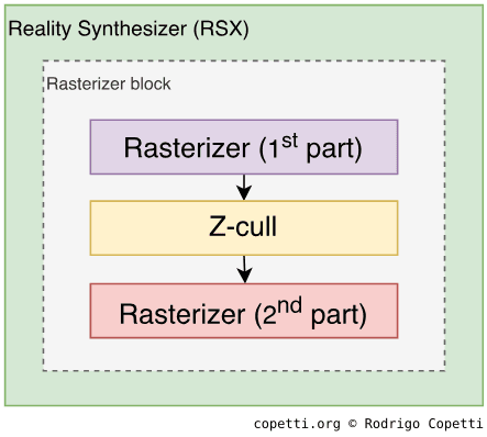
Simplified diagram of the rasterization stage. RSX embeds different units to calculate values used for interpolation of pixels and colours.
Moving on, it’s time to convert (rasterize) vertices into pixels. The RSX’s rasterizer is quite fast, it can rasterize up to 8x8 pixels (64) per cycle and works with frame-buffers of up to 4096x4096 pixels (though developers may need less than that).
The rasterizer accepts points, lines (including strips and closed types), triangles (including strips and fans), quadrilaterals and regular polygons. Naturally, as with this console generation, the rasterizer works with sub-pixel coordinates, where the sampling points are half-coordinates (0.5) of pixels. This allows the unit to apply anti-aliasing methods such as Multisampling afterwards. Multisampling consists in rasterizing the same geometry multiple times but shifting a few sub-pixels apart at every batch (the RSX supports four different shifting modes) and then computes an average. This results in a smoothed image.
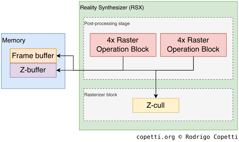
Furthermore, this unit also performs z-culling using dedicated RAM within the RSX (it has a capacity of around three million pixels). This saves processing pixels and stencils that have already been rendered and allows to perform early z-test on incoming geometry.
A separate unit is used for rasterizing 2D objects (sprites), although this one is isolated from the 3D pipeline. Consequently, RSX works in two modes, 2D and 3D, but intermittently switching between them is expensive in terms of performance.
Next in line we’ve got the Fragment Shader & Texture block, this is a programmable unit (through the use of ‘fragment programs’ or ‘shader’) that applies texture mapping and other effects.
Being an advanced successor of GeForce3’s texture units, the new block contains six fragment units (also called ‘pipes’), each one process 2x2 texels (named ‘quads’). To organise multiple units working concurrently, another sub-block called Shader Quad Distributor (SQD) is placed to dispatch quads to each fragment unit. Afterwards, each fragment unit loads the fragment program.
To compute operations, each pipe contains the enormous amount of 1536 128-bit registers. On top of all that, each pipe can process multiple quads in parallel (multi-threading), though the number of quads processed in parallel depends on the number of registers allocated to the fragment program (no. threads = 1536 ÷ no. registers reserved by shader). In global terms, up to 460 quads can be processed in parallel. Furthermore, up to three fragment pipes can process two instructions at the same time (dual-issuing, like the PPU) as long as the instructions don’t depend on each other.
The fragment units provide similar arithmetic-type instructions to the vertex unit, with the addition of texture-related opcodes, such as multiple types of texture fetching (since textures can be encoded using many structures and then compressed) and unpacking. Similarly to the vertex block, the fragment shader abides by DirectX’s Pixel Shader 3.0 model [33], OpenGL’s NV_fragment_program2 profile [34] and Cg’s ‘fp40’ profile [35]. All of this to ease programming and avoid learning low-level APIs from the ground up.
Finally, since the units will be constantly fetching texture pieces from video RAM or main RAM, this block includes three texture caches: 4 KB of L1 cache for each pipe, 48 KB of L2 cache for video RAM fetches; and 96 KB of L2 cache for main RAM. Notice that main RAM cache is significantly larger, this was a conscientious decision made to compensate for higher latency.
Before writing the results into the frame-buffer (stored either in VRAM or Main RAM), a final block called Raster Operation Block (ROP) performs final tests on the resulting pixels.
There are two sets of ROPs made of four blocks each (eight in total). Each group performs z-testing, alpha blending and the final write to memory. All in all, this circuitry can process up to 16 z-values and 8 pixel colours per clock. Curiously enough, the PC-variant Nvidia 7800 GTX features 16 ROPs instead of 8, maybe this cut was done to prioritise memory bandwidth consumed by the SPUs?
To save further bandwidth, ROPs also provide colour compression and z-compression. Additionally, there’s a Tiling mode available for optimising memory access by the video encoder. In tiling mode, the frame buffer is stored into continuous 128 B blocks ordered in the same way they would be broadcasted/scanned. Thus, saving the GPU from doing page swaps (used for memory addressing) while transmitting the frame buffer for display, consequently improving bandwidth. These ‘tiles’ are stored in marked locations in memory exclusive for this type of addressing.
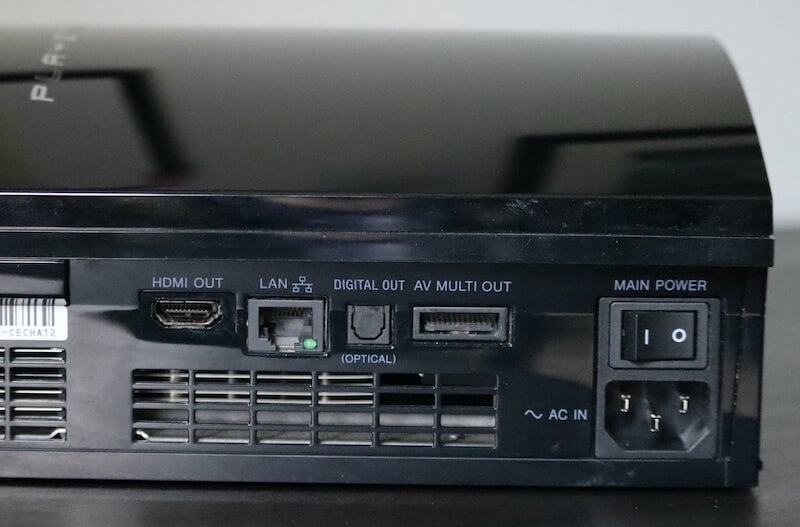
Gone are the days of console-proprietary video sockets and dozens of analogue signals squashed together in a single socket to accommodate every region on the earth. The PlayStation 3 finally incorporated a unified video signal soon to be adopted worldwide: the High Definition Media Interface (HDMI), used for transferring both audio and video at the same time.
Back of the PS3, HDMI output on the left side and at the other extreme there’s the old Multi A/V for analogue video out.
The HDMI connector is made of 19 pins [36], all in a single socket. It transfers a digital signal, meaning that the picture and audio are broadcast using discrete zeroes and ones (and not a range of continuous values found in analogue signals). Consequently, it doesn’t suffer from the interference or image degradation that previous equipment did, such as screen artefacts produced by cheap SCART cables.
To this day, the HDMI protocol is continuously being revised [37], with new versions of the specification offering more features (i.e. larger image resolution, refresh rate, alternative colour spaces, etc) while retaining the same physical medium for backwards compatibility.
Throughout the PS3 lifecycle, Sony added certain HDMI features of new revisions to the PS3 through software updates [38]. The last protocol compatible with the PS3 is version 1.4, which most notably brought support for ‘3D television’. Although, other capabilities, such as higher video resolutions, remained capped at 1920x1080 pixels, with most games rendering their frame buffers at just 1280x720 pixels.
‘Real’ 3D vision/projection
So what was that ‘3D television’ I mentioned before? Well, it so happens that the lifetime of this console overlapped with a short-lived fever for 3D tellies (the so-called 3DTV) [39]. To support these, Sony updated their SDK to assist the rendering of stereoscopic frames in RSX and implemented the ‘3D specification’ in their HDMI encoder. What’s happening behind the scenes is that the encoder broadcasts two frames at a time, and the television alternates them similarly to what the Master System’s 3D glasses used to do 30 years before.
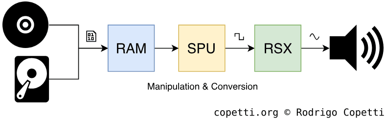
Audio
I’m afraid you won’t see a lot of information in this section anymore, mainly because since the last portable invention, audio has silently shifted to the software side. In other words, there are no longer dedicated audio chips.
You see, while the need for better graphics tends to grow exponentially (consumers want more scenery, better detail and colours), you won’t hear the same level of demands for sound. I presume this is because the capabilities have reached our cognitive limit (44.1 kHz sampling rate and 16-bit resolution). The only thing left is to implement more channels and effects, but these don’t need the processing power that would require installing specialised chips, at least with consumer equipment.
Summary of the audio pipeline.
So, in the end, audio is now completely implemented with software and processed by the SPUs (I mean the Synergistic Processor Unit, not the Sound Processing Unit! it’s a bit ironic that both share the same initials…). Moving on, Sony provides many libraries in their SDK that instruct the SPUs to carry out audio sequencing, mixing and streaming. And if that’s not enough, many effects can also be applied.
That being said, where is the audio signal sent for broadcast? The RSX. This chip also contains the ports used to broadcast raw audio signals to the TV. Before sending it, the signal is encoded in different formats, depending on the output selected (analogue, HDMI or S/PDIF, the latter is also called ‘digital audio’).
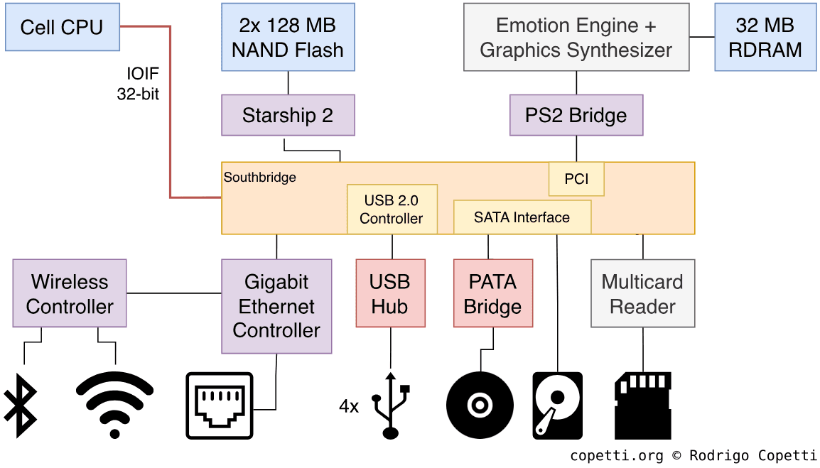
I/O and backwards compatibility
All I/O operations are delegated to another chunky chip called Southbridge[40]. This is very similar to the architecture the original Xbox adopted back in the day. It seems as if the architectural gap between consoles is becoming narrower, or maybe this approach proved very reliable and it’s architecture-agnostic, I’ll let you decide.
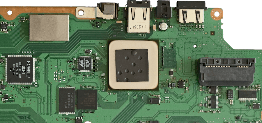
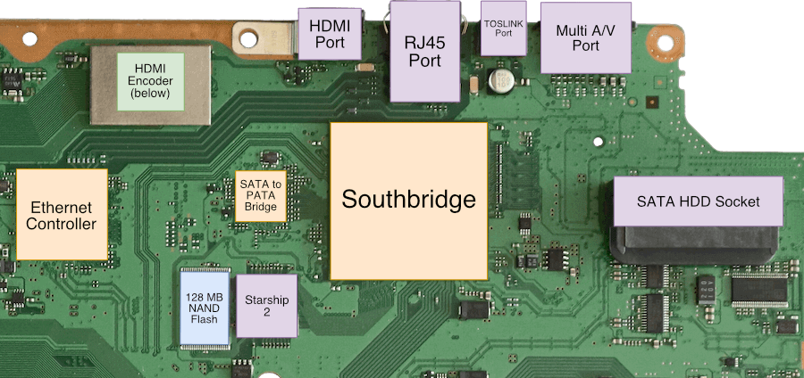
The big Southbridge chip supervising small I/O chips and interfaces.The same picture with important parts labelled.
Like the PS2’s IOP, the Southbridge is completely proprietary, though this time made by Toshiba (they called it the ‘Super Companion Chip’ [41]). So, while it still remains an obscure piece of silicon, it does a superior job consolidating many interfaces and protocols, both external (i.e. USB, Ethernet, etc) and internal (i.e. SATA). For reference, in the past, the IOP’s slow clock speed ended up bottlenecking speedy interfaces like ATA and Ethernet, greatly reducing their full bandwidth.
Furthermore, the southbridge implements encryption algorithms to protect the communication between standard protocols in a seamless way, such as the Hard Drive data.
Diagram of the Southbridge’s connections.
Overall, Southbridge embeds an enormous amount of interfaces, this has to do with the fact this console was designed during the ‘multimedia hub’ trend. It’s not enough for video game consoles to play games, but they also need to become DVD and Blu-ray players, set-top boxes (partially), photo viewers (by importing the camera’s photos using the multi-card reader) and possibly more as the needs evolve (thanks to its updatable operating system).
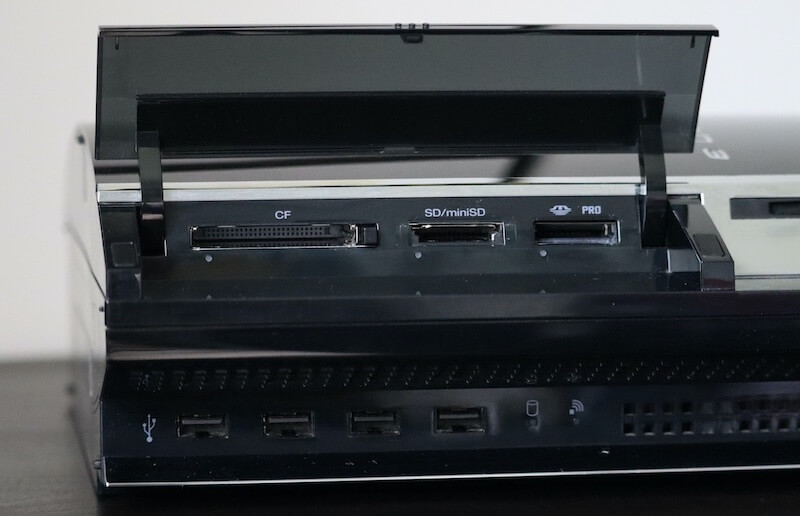
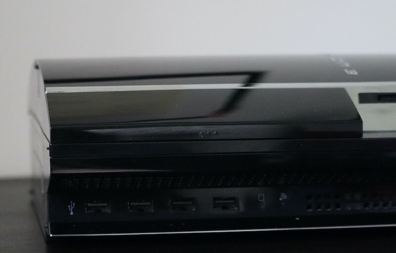
Like many PC towers of that era (including mine), a multi-card reader was in order. Next to it, you get four USB 2.0 ports. This was pretty ‘premium’ for a console costing £425! (£628 in 2021 money).Same console with the lid closed. To further cut the cost down, later models sealed the bay and removed the card reader and two USB ports.
In the case of user-accessible ports, the Southbridge is connected to:
A USB 2.0 hub: provides four front USB A ports. These can be used for accessories or to link/charge the controllers.
A Serial ATA (SATA) interface: connects the Blu-ray drive and a 2.5” Hard Disk.
Until 2008, Blu-ray readers interfaced with Parallel ATA [42], so an intermediate chip was fitted in the middle to do the SATA → PATA conversion.
1000/100/10 (Gigabit) Ethernet Controller: in the form of an RJ45 socket on the back, but it also forks to a Wireless daughterboard, providing Wi-Fi 802.11b/g and Bluetooth 2.0 connection.
A Multi-card reader: provides slots for Memory Stick, SD, MultiMediaCard (MMC), Microdrive and Compact Flash.
‘Less wire’ equipment
Thanks to wide the adoption of Bluetooth technology, wired controls are now a thing of the past. The new form of the PS2’s Dualshock 2 controller is called Sixaxis and while it’s not the radical change others decided to go for, it features a gyroscope for new types of human input. This comes at the expense of the haptic feedback (Rumble), however. A year later, Sony surprised players with the Dualshock 3, which restored the haptic motor.
On a different topic, you can now turn on the console from the wireless controller.
Internal interfaces
Regarding internal components, SouthBridge connects to:
Starship 2: an adapter for two 128 MB NAND Flash chips. Behind the scenes, Starship bridges the Southbridge’s local bus with the standardised ‘Common Flash Interface Protocol’ (widely adopted for interfacing Flash memory) [43]. The PS3 stores the operating system on these, among other things.
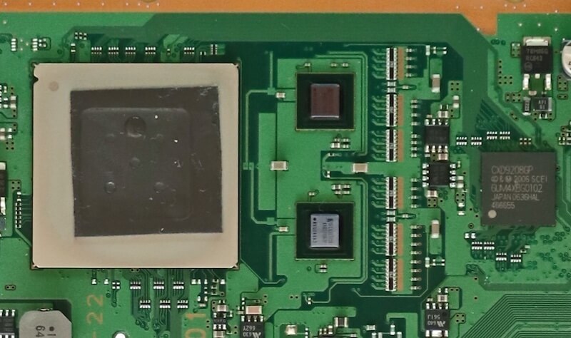
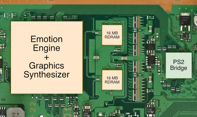
The PlayStation 2 chipset: at the corner of the motherboard there’s an eye-catching chip that houses none other than the Emotion Engine and the Graphics Synthesizer. The EE+GS combo connects to 32 MB of RDRAM and an IO bridge (named ‘PS2 bridge’), which combined form roughly 90% of the original PlayStation 2.
The EE+GS chip sends the video signal directly to the RSX.
These chips are not accessible by developers, they are used for backwards compatibility only!
Backwards compatibility
Having mentioned the PS2 chips, I guess this is my cue to talk about backwards compatibility of the PlayStation 3 once in for all.
First things first, let me introduce how backwards compatibility generally works: consoles can either play their predecessor’s games with the help of software (instructs existing hardware to behave as the old game would expect) and hardware (either the existing hardware provides total or partial backwards compatibility; and/or the company added extra chips to recreate the older system within the new motherboard). With the amount of processing power the PS3 shows, you would expect Sony to ship a PS2 emulator running within Cell and accelerated by RSX. Well, for some reason that didn’t happen and instead, Sony fitted the PS2’s chipset at one corner of the motherboard.
The big EE+GS chip, two 16 MB RDRAM modules and the ‘PS2 bridge’.The same picture with important parts labelled.
On the other side, the missing but not-as-critical chips (IOP, SPU, etc) are replicated with software running in Cell. In the case of game saves, initially, users had to acquire a memory card adaptor, but once a new software update landed, Memory Cards are now emulated as disk images stored in the hard disk, while Magic Gate (the encryption system) is handled seamlessly by one SPU.
Since the Cell and RSX are still ‘on’ while playing a PS2 game, the system offers two scaling methods for increasing the screen area during gameplay, these are ‘nearest neighbour’ or ‘smoothed’ (anti-aliased).
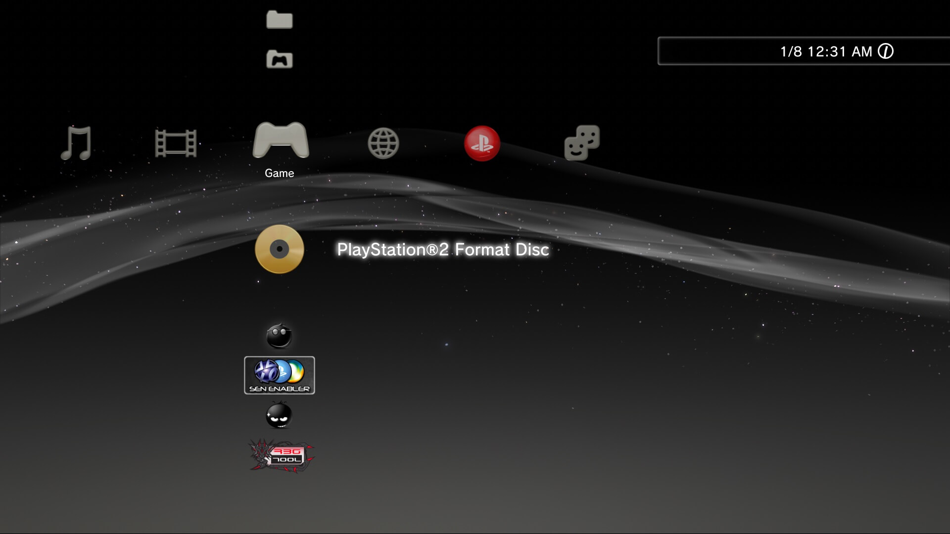
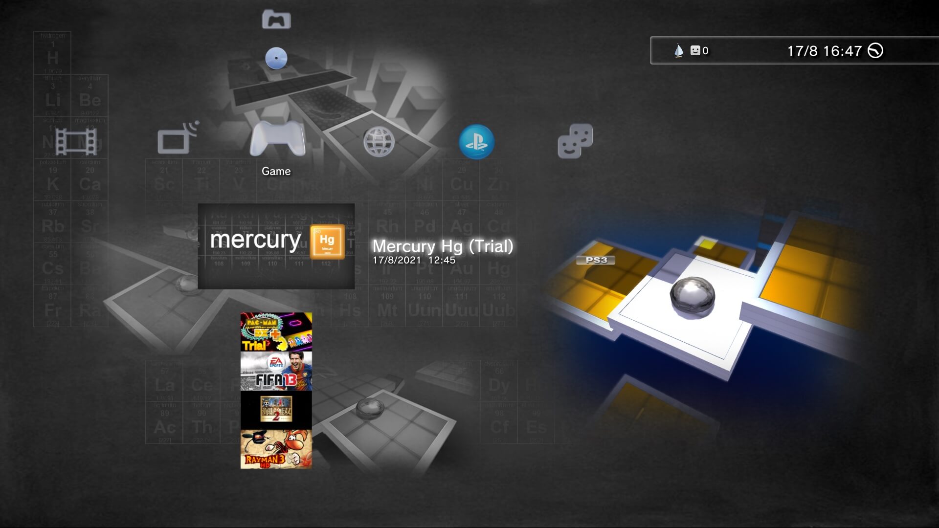
PS3’s user interface showing the game entry after inserting a PS2 disc. (Don’t worry about the other icons for now, as some are not even official).
All in all, thanks to this setup, the PS3 runs PS2 games at an impressive compatibility rate. On top of all, you can take advantage of new features that come with the new console (wireless control, HDMI interface and virtual memory cards).
As if wasn’t enough, PS1 games can run as well, this time without needing to embed the old SoC or GPU (it relies on pure software emulation).
The strange end of terms
Throughout the lifecycle of the PS3, Sony slowly trimmed PS2-only chips from the PS3 motherboard to the point backwards compatibility was solely software-emulated (with greater limitations, such as only running PS2 games purchased from their online store). Because Sony never replaced the PS2 chipset (as it had previously done with the PS1 hardware inside the PS2), it makes you wonder about the technical and executive rationale behind this. Well, as a case study, here’s my quick opinion about the reasons for this:
Timing: Sony likely intended PS2 owners to buy their new product as a replacement of their current one, as this is more affordable for consumers (they can sell their old system). However, for some reason, Sony didn’t have a software emulator prepared before release day, so they initially resorted to adding extra chips. Later on, as the software emulation progressed satisfactorily, they slowly removed these in further motherboard revisions.
To complement this, developer ‘M4j0r’ commented: “An interesting point might be that Sony developed the two hardware emulation revisions at the same time (EE/GS and GS only), I guess because some games run better depending on which you use.” [44].
Costs: The introductory price of the first revision of the console (CECHA, only in Japan and US) in 2006, which was PS2-compatible, was priced at $599.99 or ¥60,000 without taxes (£425 adjusted for 2020 inflation) [45]. The following model (CECHC, shipped in 2007 internationally) removed the Emotion Engine and RDRAM (shifting those tasks to software emulation) and launched in the UK with a £425 price tag (£603 in 2020 money). Later in the same year, Sony released a new model (CECHG) without any PS2-related chip for £126 less [46]. All this proves that backwards compatibility is, in the end, an expensive feature.
Idling hardware and wasted power: While Cell and RSX still take care of some tasks to recreate the original environment, these are minimal compared to their full potential. Combined with the fact CECHA models have a cumulative power consumption of 399 Watts [47], it does make you wonder if this design is worth the power consumption, let alone efficient (for comparison, CECHG’s new power supply consumes 285 Watts).
I understand there are other factors involved in the reduction of power consumption, like the new revisions of Cell and RSX. However, I still believe the PS2’s chipset plays an important role.
Inflexibility: The EE+GS chip is not re-programmable, which means the end result will always be the same, independently whether there are glitches or possible enhancements. Compare this to the PCSX2 emulator’s graphic enhancements [48] and its modding capabilities [49], this show us that room for improvement is possible and appreciated.
Personally, I believe pure software emulation is the most feasible option in the long term due to its scalability, customisation, and independence from proprietary hardware. But of course, this takes more effort to implement accurately, as the ongoing development of PCSX2 by a volunteer-driven community demonstrates it (please note that the aforementioned emulator only runs on x86 PCs, however).
Lateral compatibility
We are not over talking about compatibility just yet! It may surprise you that Sony also allowed users to run a subset of PlayStation Portable games as well. Though emulation was carried out completely with software, just like the PS2 compatibility in later models.
As there isn’t any UMD disc reader in the PS3, users must access a game catalogue from Sony’s online store to download and install any PSP game.
Operating System
Now that home consoles have become powerful multimedia hubs, a more convoluted operating system will be needed to provide users with more services and games with a thicker layer of abstraction. All of these, while keeping security and performance up to the task.
Consequently, terms like shell or BIOS are no longer used to describe this area, not because they don’t exist anymore but because they describe a small fraction of the new system. The generic term is now ‘operating system’, this comprises many areas (boot loader, kernel, user interface) analysed separately. As always, I recommend checking out the PSP’s OS first, since its modular design is a recurrent ingredient in the PS3.
Cell’s privileged security
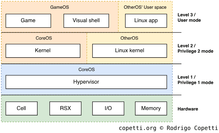
Before we dive into details, I need to mention the different modes of operation in Cell. I originally planned to describe this in the ‘CPU’ section, but since that got incredibly dense, I’ll introduce it here where you’ll see its practical use right away. Furthermore, its modes also affect the design of any operating system running within Cell - not just the one Sony developed for this console.
Having said that, to safeguard against unauthorised access to sensitive data and/or resources, Cell implements a set of privilege levels inherited from the PowerPC specification. In other words, Cell executes programs in two modes:
Privileged mode: Cell grants access to every corner of its hardware (registers, memory addresses, opcodes, etc) [50]. For security reasons, this mode should only be used by the operating system’s core (i.e. the Kernel).
Moreover, Cell was also prepared to run multiple operating systems concurrently and to achieve that in the hardware level, ‘privilege mode’ can be further divided into Privilege 1 and Privilege 2. ‘Privilege 2’ is meant to be used by a Kernel, while ‘Privilege 1’ is used by a Hypervisor, the latter arbitrates resources between different Kernels running at the same time.
The ‘hypervisor’ functionality also turned into an area of research in IBM’s headquarters [51][52].
User Mode: As the name indicates, Cell only grants a limited set of resources [53] and it’s directed to traditional applications running on top of the operating system. If for any reason, a program requests access to a protected location, then execution jumps to the Kernel or Hypervisor to request whether access should be granted or not.
Additionally, SPEs contain a modus operandi called isolated mode and it shields the execution process within the SPU so no external unit (the PPE or other SPEs) can access it until the SPU finishes. This can be activated after uploading a program to any SPE and ensures that the processor is not tampered with while the sensible code (i.e. an encryption routine) is being executed.
Sony’s operating system, which I’m going to describe in the following paragraphs, uses all the modes described to handle its security.
Overview
As I said before, the OS is quite complex. So, to be able to follow this section without too much trouble, we can divide the type of files we’ll find in the operating system of this console into different layers:
Loaders: to make a long story short, programs/binaries in this console are systematically encrypted. So, ‘Loaders’ are programs that execute ‘real’ programs. To put it in another way, Loaders grab binaries, decrypt them, check their authenticity and finally send them to the respective processor (the PPE or either SPE) for execution. If that doesn’t sound complicated, Loaders are chained together to protect the software even further. Finally, Loaders are found across many media.
Some Loaders are updated by Sony (through software updates) while others can’t be changed. This is independent of whether they are installed in re-writable storage, as some loaders are encrypted using console-specific keys, so they can’t be altered after the console leaves the factory (at least through traditional means).
System files: these comprise low-level binaries (executed through Loaders), metadata for organising the hardware, utilities and other assets (i.e. fonts, imagery). Just like Loaders, there are console-specific system files that cannot be replaced or autogenerated.
Some binaries borrowed code from the Free BSD and NetBSD projects [54].
User Content: These include configuration files (i.e internet settings), data used by games (i.e. game installation files and saves) and data generated automatically by the console (i.e. hard drive information).
Unlike the other layers, destruction of this data does not lead to catastrophic outcomes.
OS’ security hierarchy
Generally speaking, the PS3’s OS is designed with the same modular approach as the PSP. To recall the previous article, the OS is made of multiple modules. These may serve the user (like a game or app) or reside in memory indefinitely to serve other modules (in the form of system calls and/or drivers). Some modules have more privilege access than others (kernel module vs. user module).
Diagram showing how the components of the PlayStation operating system fit in Cell’s privilege levels. References to ‘OtherOS’ are explained further in the next sections.
The operating system, throughout its lifecycle, will call upon many modules with different privileges. Sony constructed its OS so that modules run under Cell’s three privilege levels:
Level 1: here is where a Hypervisor programmed by Sony resides. Also referred to as lv1, this program is the door to every single bit of this console and chained to exceptions triggered by the MMU. That being said, the hypervisor only accepts requests from programs authorised by Sony (residing in the next privilege level). While the Hypervisor resides in memory, it also provides low-level system calls and FAT16 filesystem support.
Level 2: naturally reserved for the Kernel, a privileged program also named lv2 or ‘Supervisor’. The kernel abstracts the hypervisor so level 3 programs don’t interact with it directly. The Kernel provides multi-threading functions for both PPU and SPU. Ultimately, the Kernel bootstraps userland modules.
Level 3: the rest of the programs (called userland or userspace), including games and the visual shell, run at this level. These plebs are under the will of the Kernel to communicate with the console’s hardware and cannot spawn any new process or program unilaterally.
Storage medium
With all being said, where is all this data stored? From a general user’s perspective, there are only two visible media: Blu-ray discs for games and a Hard Disk for saves. Well, there are a few more, so we will now examine every one of them!
It turns out, within Cell there’s a small ROM hidden somewhere that manufacturers may store a ‘protected’ boot-loader. IBM provides this space to spare any company (not just Sony) from having to manually implement tailored obfuscation methods to protect their boot code, as off-the-shelf components are not always prepared for bespoken needs.
Since this piece is already physically protected with obfuscation, it doesn’t have to be encrypted. Thus, it’s ideal for a first-stage boot-loader (which can’t be encrypted) and the PlayStation 3 stores its early boot stage there.
Remember about those 256 MB of NAND flash I briefly mentioned before? Well, here is where most of the operating system resides. That is, until Sony released the CECHH model in late 2007, replacing the 256 MB NAND for a puny 16 MB NOR. As a consequence, some files had to be moved elsewhere. For the sake of simplicity, let’s first see what these chips store [55]:
Console-specific Loaders: specifically, two loaders called bootldr and metldr. These files are encrypted with a key engraved during manufacturing, so they can’t be replaced!
Be as it may, there are hidden functions in Sony’s hypervisor that allow to update these, although, for some reason, they have never been used [56].
CoreOS: the first half of the operating system. It mainly consists of more loaders that will continue the boot process and eventually bootstrap the second half (GameOS). CoreOS also supplies the Recovery Menu, an alternative shell that contains maintenance utilities that users can use to (attempt to) repair their console.
Unique IDs: similar to the PSP’s IDStorage, these are used by the console to control secured hardware like the Blu-ray drive; or by Sony to authenticate the console with their online servers (i.e. the IDPS key).
Security assets: some programs depend on them to perform security operations. For instance, Blu-ray movies with DRM check a block called Virtual Table Rights Management (VTRM). Sony also stores revocation tools and records to blacklist security certificates that have been compromised in the past.
Due to their larger size, models with NAND Flash also store the remainder of the OS (called GameOS or devflash). This includes:
The Visual Shell (VSH): a continuation of the PSP’s signature interface, it’s also bundled with tons of modules (plugins) and assets.
Emulators: aforementioned programs that enable a PS3 to run PS1, PS2 or PSP games. The specific PS2 emulator loaded depends on the console revision (whether it has full PS2 hardware, partial hardware or uses no PS2 hardware whatsoever).
Runtime libraries: programs developed with Sony’s SDK are dynamically linked to a set of libraries stored here.
Blu-ray Player: programs that handle interaction with the Blu-ray drive and movie decoding.
System assets: such as fonts and certificates that binaries depend on to work.
As if it wasn’t enough, NAND consoles also house other data like the xRegistry (collection of network settings, PlayStation Network accounts and a list of Bluetooth-paired devices), more revocation records and a Loader for OtherOS (a really interesting piece which we’ll discuss more in the next paragraphs).
The debuting 2.5-inch Hard drive, ranging between 20 GB and 500 GB (as more revisions were shipped), provides persistent data storage for:
User content: including game saves, trophies (more information in the ‘Games’ section) and other user-related data.
Game assets: games can copy files from the disc to the hard disk to improve loading times. These are treated as ‘game data’ by the operating system.
Cache: a separate 2 GB partition is available to games for temporary storage (in case main RAM is not enough).
NOR systems, however, also store GameOS in the HDD. As a consequence, whenever the user swaps out the hard drive, the console asks for an update file to re-install GameOS into the disk. Be as it may, neither NOR nor NAND systems will boot without the hard disk.
Certain user data can be backed up using a USB stick and then moved to another console if necessary, though this process re-formats the newer console before copying the old data.
In 2012, Sony unveiled a redesigned revision of the console called ‘SuperSlim’ (codenamed CECH-4xxx). These were available in three flavours: One with a 250 GB Hard drive, another with a 500 GB Hard drive, or a third option with only a 12 GB eMMC internal flash. The first two options follow the file system layout implemented in NOR models, while the third one stores everything in the eMMC (including user data) and follows the NAND layout to store system files.
There’s a catch in the eMMC model, however. In the place of the NOR chip, Sony fitted a Panasonic ‘MN66840’ chip which, according to the PS3 Dev Wiki [57], it seems to redirect the NOR bus to the eMMC. I assume this is just a trick to save costs, as it recycles the same Southbridge from the other variants.
Curiously enough, if the user decides to fit a Hard Drive into the eMMC model, the console moves all user data away from eMMC to the new Hard drive. As a consequence, the user can fully utilise the hard drive, though the empty space in eMMC is now left to waste.
All right, using all the previous knowledge, you are going to learn now how the system boots up - and let me tell you, it’s pretty complicated. The reason is simple: Sony doesn’t want you fiddling with their hardware or software, so they built many layers of obfuscation and encryption to prevent you from breaking in and side-loading your own code (and hopefully give up and keep buying games/movies/whatever) but, as history will tell you, the opposite happened.
In the following section, I’m going to describe what this console does once you push the power button. Note that this process only drastically changed once (after hackers cracked it). So, for simplicity purposes, we’ll start with the ‘original’ boot process (implemented before system version 3.60)[58][59][60]:
A separate chip in the motherboard (called Syscon) powers on and executes instructions from its internal ROM. It then sends a ‘Configuration Ring’ to Cell via SPI (a serial connection), this initialises Cell and deactivates the eighth SPU. Finally, it latches the power line and gives life to Cell.
Cell’s PPU reset vector points to its hidden ROM, which stores the routines to locate and decrypt bootldr from Flash. The decrypted piece is then loaded by the first SPU in isolation mode.
The now-isolated SPU, having loaded bootldr, initialises part of the hardware (XDR memory and I/O interfaces) and decrypts a binary named lv0 and instructs the PPU to run it.
The PPU, now executing lv0, decrypts metldr (a console-specific loader) and sends it to the third SPU, again in isolation mode.
The SPU2, now executing metldr, executes five more loaders sequentially:
lv1ldr decrypts and loads lv1, which contains the Hypervisor that takes over the first privilege level. Moreover, lv1 sets up the hard drive, Blu-ray drive and RSX.
lv2ldr decrypts and loads lv2, which contains the kernel and runs on top of the hypervisor. It also finishes initialising RSX, the PS2 emulation, Bluetooth, USB controller and the Multi-card reader.
appldr decrypts and loads vsh (the Visual Shell) and other dependencies. vsh will later enable the user to load a game.
isoldr decrypts and loads modules that will run in the third SPU in isolation module. These modules are critical for security and perform many cryptographic functions throughout the console’s lifecycle. Consequently, the third SPU is reserved for security functions and games can’t use it (leaving only six SPEs for games).
The PPU, having loaded vsh, grants the user control through a graphical user interface, which manifests itself with an iconic orchestral splash sound followed by the XMB menu.
Revisioned boot process
In March 2011, a hacker known by the name ‘GeoHot’ broke the security of metldr, thereby compromising the authenticity of subsequent loaders. Thus, Sony retaliated by issuing security updates for both their hardware and software. These fixes are further discussed in the ‘Anti-piracy’ section of this article.
Visual Shell
Are you getting tired from all this theory? Let me switch to something everyone can actually see: The Visual Shell.
XrossMediaBar (XMB), a new user interface that gained international recognition two years before, has been slightly adapted so it can be interacted from the sofa (the so-called ‘10-foot user interface’) and expanded to take advantage of ‘full HD’ resolution (1920x1080 pixels).
XMB in the PSP (2004). Rendered at 480×272 pixels.XMB in the PS3 (2006). Rendered at 1920x1080 pixels.
While PSP users will find many familiarities, Sony added a new set of apps that use the potential of Cell, RSX and the Blu-ray drive. Many of them related to multimedia (i.e. video player and image slideshow), television (such as on-demand TV apps, like BBC’s iPlayer), social profile (online avatars) and online purchases (PlayStation Now and PlayStation Store, to name a few).
Additionally, since this is a home console that might be shared by multiple members, XMB supports multiple users, where each one may use a different PlayStation Network account and store separate user data (purchased games and saves).
Just like in the PSP, highlighting a game may style the background to get your attention!.The XMB provides an immense amount of settings, especially helpful when you need to setup your shiny new 1080p telly with 3.1 surround audio.Various multimedia options.XMB can install games, updates and expansions (DLCs) using a native package installer.The PlayStation 3’s XrossMediaBar (XMB) interface
Finally, the inclusion of a hard drive is a relief for the veterans that in the past were obliged to buy expensive proprietary storage (Memory Stick Pro Duo) whenever they ran out of space.
Lend me your PS3
Impressively enough, not every app bundled with this console had self-interest goals. With the advent of distributed computing and the capabilities of Cell for data science projects, Stanford University joined hands with Sony to enable PlayStation 3 owners to contribute to medical research. The result was Folding@home (pronounced ‘folding at home’).
Folding@home was an application installed in every PlayStation 3 that, once opened by the user, connected to a central server and ran protein simulations. Moreover, the app was also allowed to run in the background during off-peak times.
Folding@home displaying the work accomplished since the user started the app [61].
Throughout its lifetime, the joined computing power of 15 million PS3 users worldwide assisted Folding@home with their research towards curing Alzheimer’s disease [62]. In the end, Folding@home and Sony retired the app in 2012 and the former lives on on other platforms.
This is my personal opinion, but I enjoy reading about projects that make global contributions using the capabilities of distributed computing, as opposed to the never-ending sensational articles wining about cryptocurrency mining. I guess we shouldn’t forget that, with every new powerful technology, there will always be selfless applications developed for it.
A multi-OS proposal
When IBM described Cell from the software level, they mentioned that Cell is capable of running multiple OS at the same time, due to Cell’s many execution cores [63]. Thus, Sony took this idea forward and added an option in XMB to install a secondary operating system[64]. This feature was called OtherOS and, in a nutshell, provides a partition manager (XMB just guides the user to resize GameOS’ partition and allocate new space for the second OS) and a button to boot from the second OS (thanks to OtherOS’ boot files already setup in Flash). So, the user just need to fill the new partition with an OS. Consequently, many Linux distributions (i.e. Ubuntu and Fedora) added the PS3 as another possible target to install it on. You may consider this a spiritual successor to Linux for PS2.
Red Ribbon GNU/Linux is a distribution exclusive for the PS3/Cell and compiled using the PPC64 target [65].
Thanks to OtherOS, experienced users had the opportunity to develop homebrew applications running on Cell without licensing restrictions, this was particularly interesting for research/scientific purposes [66][67], as this console carried a more affordable price tag than a mainframe. For multimedia purposes, the Blu-ray drive and Multi-card reader were also accessible from OtherOS.
On the other side, while OtherOS’ privileges may surpass GameOS’ (at the kernel level), they don’t overtake the hypervisor, which still resides in memory. So, any hardware access from OtherOS still depends on the will of Sony’s hypervisor, and it so happens that the latter blocks access to RSX’s command buffers (preventing the use of the shader units, among other components used for accelerating graphics operations). Consequently, resulting Linux distribution resort to software rendering (all graphics are drawn by Cell) and then stream the frame-buffer to the RSX for display. While it’s disappointing that OtherOS can’t make use of the full capabilities of this console, this was probably done to reduce attack surfaces. Ironically, OtherOS’ use of Cell is similar to how IBM/Toshiba/Sony may have originally envisioned the PS3!
Sharing the same fate of Folding@home, OtherOS was eventually removed in a subsequent update, but due to different causes (mainly related to security). Shortly afterwards, OtherOS was unofficially restored thanks to software exploits and reverse engineering efforts. At the moment, OtherOS is available if the user installs a custom firmware. I explain this further in the ‘Anti-piracy and homebrew’ section.
At the time of this writing, developer René Rebe is currently implementing proper xf86 drivers that take advantage of the acceleration provided by RSX and its 256 MB of memory [68]. His work is combined with other developments that removed the restrictions imposed by the hypervisor (initially thanks to the discovery of software exploits and later with the use of a custom firmware, the latter is explained further in the ‘Anti-piracy and homebrew’ section). Mr. Rebe publishes his progress on his Youtube channel and relies on voluntary donations to continue his work [69].
Updatability
For the final part of this long section, let’s talk about the updatability capabilities of GameOS.
In a nutshell, just like the PSP, Sony distributed PS3UPDAT.PUP files that package all the new OS binaries. Due to the console’s security system, only those files which aren’t secured with unique console keys and are stored in re-writable storage (Flash, Hard drive, eMMC) are updatable, the rest must stay as it is.
PUP files were distributed through Sony’s official website, the XMB update assistant or found in the contents of a game disc (all games embed a PUP file, reflecting the SDK version developed for). Since models with NAND Flash contain only 256 MB of space and store the whole OS there, Sony never released update files with sizes higher than 256 MB.
Games
This section encompasses topics related to game development, distribution and services.
Development ecosystem
As this console amalgamates technology from various companies, including products already commercialised in other markets (i.e. Nvidia’s GeForce7 GPU line for PCs), developers were drowned with many different tools to develop their software. Note that this doesn’t imply development was easy, but it’s something to appreciate compared to the assembly days.
To program Cell, IBM and Sony shipped separate development suites, IBM ones targeted non-restrictive environments like Linux (and OtherOS), while Sony’s tools explicitly targeted the PS3’s GameOS as the only execution environment.
Having said that, IBM distributed the IBM Cell SDK package for free [70]. It includes the GCC toolchain modified to generate PPU and SPU binaries, allowing development in C, C++, Fortran and assembly. It’s also cross-platform, enabling to compile code from other equipment (like an x86 PC). The SDK also included low-level libraries to facilitate SIMD mathematical operations and SPU-PPU management. Finally, it bundled a fork of Eclipse IDE.
To ease the complexity of Cell development, IBM also developed another short-lived compiler called XLCL that compiles OpenCL code (C/C++ variant for parallelised computations) for the PPU and SPU. Though this was only distributed through IBM’s Alphawork’s channel, meaning it remained experimental.
Now, what about Sony? Well, similarly to their PSP SDK, they shipped hardware devkits (many variants with different sizes and enhancements) and a software package made of compilers, libraries and debuggers that used Visual Studio 2008 (and later 2010) as an IDE [71]. Since they only supported the PS3, their SDK included the same GCC toolchains but complemented with tons of libraries to assist in graphics tasks, audio and I/O. In the case of graphics/RSX, Sony provided GCM to build raw commands and psGL, built on top of GCM, to provide an OpenGL ES API. To write shaders, Nvidia provided Cg, a shader compiler that parses a language similar to HLSL (the shader language defined by Microsoft).
License-free development
With the advent of native Homebrew (running on GameOS, not OtherOS), new open-source SDKs were created to bypass the dependency of Sony’s copyrighted libraries and therefore prevent copyright litigation. One example is PSL1GHT, an SDK used in conjunction with ps3toolchain[72], to provide a full development suite ready for developing legal Homebrew (though this requires a modified/hacked console with signature checks disabled).
Back in 2018, I built my own suite based on ps3toolchain but distributed in the form of a Docker container [73], so developers wouldn’t need to compile ps3toolchain and instead download my pre-compiled setup (saving many hours of compilation time). The container also bundled many tools like Nvidia’s Cg shader to mitigate dependency problems that I found while experimenting with PSL1GHT-based project. In the end, it was a fun experiment that helped me learn more about the development environment.
Outsourcing development
It’s worth pointing out that a peculiar business-to-business model raised in popularity during that time: Game Engines. Instead of spending time and money developing a game from the ground up, why not buy the codebase of other companies and build the game on top of that? This is what game studios like Epic Games envisioned [74]. Apart from selling popular game titles such as Unreal Tournament 3, the studio licensed a stripped-down version (without the assets) to other developers. This was packaged and named ‘Unreal Engine 3’. In a nutshell, game engines take care of all the fundamental areas (physics, lighting, etc) so developers only have to add their custom content (scripts, textures, models, sounds, etc.).
Game engine licensing is not a new business model, but due to the challenging environment of the PS3, they eventually became another attractive option for development.
Storage Medium
Now that we’ve finished talking about game development, it’s time for distribution. So, here I describe the official distribution mechanisms available for PS3 games.
New generation = new medium. As the advantages of DVD start to wear down and its limitations, expressed by the game industry (space limit) and the film industry (480i format) [75], become apparent, it’s a matter of time before Sony unveils another standard to replace their new appliances. For this new console, the Blu-Ray disc was chosen.
The Blu-ray, as the name indicates, is a new optical disc format that delivered higher storage density thanks to the use of blue light diodes[76], as opposed to red diodes used with DVDs. Since blue light has a shorter wavelength than red light, more information (pits and lands) can be squashed together in the same space [77]. As a result, Blu-ray discs provide a surprisingly large capacity (between 25 GB and 50 GB!) using the same plastic disc with the same dimensions as the CD/DVD.
The Blu-ray data format responds to many needs by different industries: high definition film, digital rights management (DRM), region locking, a new file system and even a runtime environment for Java programs [78]. In the case of the video game industry, retail games for PlayStation 3 were distributed in 25 GB or 50 GB Blu-ray discs with copy protection. These are read by a 2x drive reaching speeds of up to 8.58 MB/sec [79], though the PS3’s laser can also read DVDs (at 8x speed) and CDs (at 24x speed) to play old games and movies.
While launch titles execute from the disc, later games copied part of their assets to the Hard Drive to increase reading speeds. Nevertheless, the game disc is always needed to kickstart the game.
The PS Store app in XMB.Games catalogue shown upon opening the store.The search interface (which bypasses XMB’s native keyboard, by the way).Example of game entry (accompanied by suggestions that only work on other consoles…).
At the same time of the console’s release, Sony launched its proprietary distribution channel called PlayStation Store, allowing game studios to sell their games digitally and users to purchase new content without leaving their sofa. These don’t require any physical medium to work (apart from space in the hard drive) but the digital product’s ownership is tied to an online account, something that became a concern for users in March 2021, when Sony announced [80] (and later retracted [81]) the closure of this store.
Within their digital store, Sony also took the opportunity to sell digitalised versions of PS1, PS2 and PSP games called PlayStation Classics. These are also downloaded and installed in the same way, but use the bundled emulators to work. In fact, PS2 classics invoke the same unaccelerated software emulator independently whether the PS3 models contain the PS2 chipset [82]! I guess this is the closing chapter for hardware-based emulation in the PS3.
Behind the scenes, the PS Store is just a website only accessible through the PS Store app in XMB. Throughout its lifecycle, its user interface has been revamped a few times to reflect what I suppose was a global demand for more fancy user interfaces.
Apart from the online store, there were many more online solutions added to the platform, including the debuting PlayStation Network, a free online service competing directly with Microsoft’s paid-for Xbox Live.
PlayStation Network enabled users to create a personal account and assign an avatar, then use that new digital persona to do multiplayer gaming, message and other social interactions. Users can also earn trophies if they complete a certain event in a game, and these then show up in the online profile (as in some form of medal of honour) to intimidate rivals and gain the respect of friends, I think.
Games offer an achievement catalogue to challenge their users. The intent is to provide players with a sense of pride and accomplishment.Friends list. (Names are redacted for obvious reasons).After doing some online gaming for a bit, random people started sending me messages.
Last but not least, just like having an updatable operating system, games are updated too. Hence, upon launching a game, XMB may suggest downloading game updates (in the form of ‘packages’) that patch glitches and/or add new content. Updates install in the hard drive and work similarly to a layered file system.
Anti-Piracy and Homebrew
Everything you’ve just read has to be protected somehow against ‘unauthorised’ access. If you want to know an overview of how Sony carried out that, you are in for a treat.
Security foundation overview
Many parts of the console already provide security features that don’t require any manual implementation in software:
SysCon, the obscure proprietary chip (briefly mentioned in the boot process), controls the power lines of Cell, RSX and Southbridge. Its EEPROM contains records read by the operating system’s modules to determine which functions are enabled and which are not [83].
Though I use the word ‘obscure’, SysCon is just a microcontroller, either an off-the-shelf ARM7TDMI-S (that’s right, the PS3 shares some of its DNA with the Game Boy Advance and even late PS2 revisions) enhanced with MagicGate support, or a custom NEC 78K0R variant [84]. SysCon’s internal firmware is what intrigues the most.
SysCon and Cell communicate to each other using a serial interface (SPI) which plugs to Cell’s TEST component [85]. TEST provides many debugging functions on Cell, although SysCon only connects to the ‘Pervasive logic’ port, enabling SysCon to manage areas like power or thermal [86].
Cell houses a hidden ROM that store unencrypted boot routines without worrying about snoopers.
Cell’s privilege modes and SPE’s isolated mode prevents programs from accessing unauthorised resources.
The Southbridge seamlessly encrypts the hard drive’s content using AES.
The Blu-ray subsystem is another walled fortress, and its disc content is encrypted using a key found in the ‘ROM mark’ area of the disc (inaccessible by conventional readers) [87].
On top of this, Sony implemented the following protections in software:
A complex Chain of trust that starts with Cell’s unencrypted boot ROM and ends with a graphical user interface (XMB) that only loads encrypted binaries (by Sony) under a kernel and hypervisor.
The chain of trust implements multiple encryption algorithms, including asymmetric ones like RSA and ECDSA and symmetric systems like AES; combined with HMAC and SHA-1 (to confirm the integrity of data).
Some encryption keys are produced during manufacturing, meaning if hackers find and leak these keys, they will not work on other consoles. Though this comes at a cost of Sony not being able to patch software encrypted with those keys once the console leaves the factory.
These special keys are used for bootldr and metldr (the early boot stages).
Games must call the kernel to access the hardware, which in turn asks the Hypervisor. This ‘abstraction onion’ prevents game exploits from escalating privileges, in theory.
Defeat
You’ve seen how much this console is capable of, did you expect hackers to settle with the limited features of OtherOS? I guess Sony didn’t either, the company tried hard to protect some areas, while leaving others half-closed, as hackers will later demonstrate.
Let’s take a look at how some of its strongholds were cracked by independent hackers across the world, bear in mind the PS3 hacking community was very active, with many tools and documentation produced every year. So, I’m going to focus on a few milestones that pave the way to an influx of content and homebrew development, but you can find more info at PS3History [88].
In 2010, after three quiet years in the hacking scene, the community took a turn for the best. George Hotz, a hacker known for previously unlocking the first iPhone model (a.k.a the ‘2G’) so it can work with any network (originally only on Cingular/AT&T), managed to read and write protected areas in memory without being stopped by the Hypervisor. He then published his exploit along with a short summary in his blog [89].
The exploit requires two materials: A Linux installation running under OtherOS (for arbitrary, yet limited, code execution); and an external glitcher connected to the XDR bus (interfacing main RAM). To make a long story short, the hypervisor uses a hash table stored in main RAM to catalogue memory addresses along with their privilege levels, so user programs can’t access protected memory spaces. The attack works by breaking the integrity of such table to be able to write over it, and then use that privilege to modify the entries to grant the current program access to every corner in memory.
In summary, Hotz discovered that under Linux/OtherOS, programs can request the Hypervisor many blocks of memory pointing to the same physical address, but if the program deallocates them while there’s an external interference in the XDR bus (due to a glitcher sending electrical pulses), the deallocation process ends half-done [90]. As a consequence, the hypervisor’s hash table (residing in RAM) still contains an entry of the allocated addresses, but at the same time, it thinks that that space has been freed. Hotz’ exploit then proceeds to request more blocks so the Hypervisor extends its table with more entries, and the process continues until an entry of the hash table overlaps the memory location of the block that was supposed to deallocate. Since the hash table kept the old entry granting the user access to that address, the hypervisor ends up giving the user access to modify a hash table entry! Thus, the exploit amends the entry to extend access to all memory space.
While this exploit required a Linux-running-under-OtherOS environment, it was a huge step towards further reverse-engineering and research projects, since hackers were now able to investigate critical areas of the system that were originally inaccessible. It’s worth mentioning that, during the same time, Sony released software update 3.21 removing OtherOS. You would think that this would deter hackers from continuing their work, but it just gave them more reasons to speed it up.
Later in 2010, a group identified as ‘PS Jailbreak’ announced (and later released) a unique solution to run Homebrew directly from the console’s native shell (XMB, under GameOS) without requiring to tamper with the console’s hardware. All of this at the dismay of Sony, who will soon take the legal route to block sales of that product.
‘PS Jailbreak’ consisted of a USB dongle that was plugged into the front USB port before the console was turned on. The user would then have to press the power button and shortly after, the eject button. If the instructions were carried out successfully, users would then see the normal XMB interface but with the addition of an ‘Install PKG’ option and a couple of homebrew apps made to dump Blu-ray games into the hard disk, and then load them.
Behind the scenes, this dongle carries out a huge amount of work, which can be divided into two groups [91]:
The USB exploit: Once the console is turned on, the dongle tricks the system into thinking it’s connected to a six-port USB hub, and then performs a complex sequence of USB commands until it reaches a heap overflow and escalates access to the PS3’s Kernel (level 2), it then proceeds to execute a payload.
The Payload: this is another complex package that patches the original shell to enable hidden functions only available on debug units (i.e. the ‘Install PKG’ entry), disable signature verification (to load any arbitrary module/package); and redirect Blu-ray commands to the hard drive instead (for loading games from the hard drive). The fact this program can alter so much from the kernel level makes you wonder what’s the hypervisor good at?
To complement this, I was later told by M4j0r: “Interestingly it doesn’t even exploit Sony’s code, this part of lv2 was written by Logitech and the developers of that exploit might had access to the source code (due to the 2008 hack).” [92].
This product was subsequently reversed-engineered by other communities and shortly after, open-source clones appeared (i.e. PS Groove) which removed many restrictions (for instance, users could now unplug the device after the exploit finishes). Some forks were even deployed on a Texas Instruments calculator [93]. In any case, Sony acted quickly with software update 3.42 to remove this gold mine [94], although the door for Homebrew was already opened.
Before I finally talk about the grand prize of the PS3 homebrew scene, let me describe to you a couple of methods that were developed around the same time:
The USB Jig: another USB stick, this time programmed to trick the console into entering Factory Service Mode, which is only intended for servicing the console by authorised personnel. The program embedded in the Jig replicates what Sony provides to their engineers. The main advantage of service mode is to enable to downgrade the console to a PSJailbreak-compatible version. The payload was also available in the form of a Homebrew app for the PSP [95]. Sony responded by patching service mode to make it harder to restore it to ‘normal’ mode or alter the firmware from it, discouraging users from resorting to Service mode.
The Optical Disc Emulator (ODE): a series of hardware products that different companies (Cobra, E3, etc) shipped. Instead of tampering with the console’s firmware, these tampered with the Blu-ray’s SATA/PATA interface. ODEs are boards that sit between the motherboard and the Blu-ray drive, thereby acting as a middleman that tricks the console into thinking it contains a valid disc game, but it’s instead loading a disc image from an external USB drive. The hacking history of the PS3 contains long gaps of ‘unhackable periods’ where there was no software exploit available for new consoles. So, at a hefty price tag, ODEs came to fill that gap.
The Downgrader: as Sony kept mitigating exploits with more software updates, users were left with no viable options but to downgrade to an exploitable firmware. Thus, there were companies like E3 that shipped specialised equipment that could overwrite the console’s system the ‘hard way’. That is, by directly flashing the NAND or NOR chips. For obvious reasons, this method required more skill and patience compared to the USB-based ones.
Isolated leaks: this one is for research purposes, as opposed to a ‘feature’ the user will see (but imperative for further developments, nonetheless). Anyway, the revocation data (used to blacklist compromised certificates) is parsed by lv2ldr, so far so good? Well, it was discovered that this process contained many vulnerabilities. Firstly and for some unexplained reason, revocation data is writable in userland. Secondly, the parser doesn’t perform bounds checking on the data fetched (here we go again). Therefore, hackers managed to craft custom revocation data that could produce a buffer overflow and ultimately enable them to run arbitrary code inside the SPU’s isolated mode. This allowed them to get access to confidential data (i.e. keys) that was presumably protected from the rest of the system [96].
Just like the PSP saga, the initial exploits required a lot of effort and could be easily patched by Sony, thereby resulting in a disadvantageous cat-and-mouse game. However, as it happened with the PSP, it was a matter of time before a discovery broke the fundamental security of this system: its chain of trust.
In 2011, George Hotz (along with the fail0verflow team) published another breakthrough, the private encryption keys that Sony uses to sign binaries executed by metldr. Binaries loaded during that boot stage are signed with an ECDSA key. Being an asymmetric encryption system, this means that anyone that possesses the private key (Sony, and now others) can encrypt and sign binaries, consequently, they will look ‘authentic’ in metldr’s eyes. Since metldr is the third boot stage before loading lv1 (the hypervisor), this means hackers will be able to customise or develop their own hypervisor, kernel and anything underneath it. On top of that, every PlayStation 3 in the market will also think the custom binaries are authentic. All in all, a Pandora-style exploit completely done with software.
The discovery of this key, which should have been computationally unfeasible, is possible thanks to what is considered a ‘blunder’ in Sony’s implementation of the ECDSA algorithm. To make a long story short, the mathematical formula used for ECDSA uses a random value which Sony never changed in all the update files they distributed [97], turning that number into a constant, thereby making it easier to solve the other variables, which is what happened eventually.
The effects of this discovery are described in the next paragraphs.
Cracking metldr meant everyone was now able to create ‘official’ systems for the PS3, this resulted in an influx of GameOS ‘flavours’ which different communities produced with various customisations. These systems were modifications of Sony’s official firmware files (that Sony distributed as updates) and re-packaged using Sony’s leaked keys, so they could be installed anywhere. The result was called Custom Firmware (CFW) and became the de-facto method for hacking this console, that is until Sony responded with tough measures.
My CFW installation with ‘VSH menu’ opened. This variant (called ‘Rebug’) also enabled me to turn my console into a debugging station (notice the IP address at the bottom right corner, you need to enter it on the debugger to attach to a running process) and fiddle with my own homebrew.
In the meantime, many CFW appeared on the net with many names (i.e. ‘Rebug’, ‘Ferrox’, etc) and they contained customisations such as [98]:
Disabling signature verifications on any module installed or to be installed.
Enabling to read and write (the classic peek and poke) over any memory address, either using the Hypervisor (level 1) or the Kernel (level 2).
Activating hidden debug functions to install modules packaged as ‘pkg’ files. These didn’t need to be signed with Sony’s keys to work inside a CFW environment.
Enabling to mount disc images as a virtual Blu-ray disc.
Restoring OtherOS and even enhance it by removing the restrictions imposed by the Hypervisor. The result was called OtherOS++.
Writing over Syscon EEPROM’s database to enable to install any system version of choice. This is also known as QA Toggling.
Altering the style of XMB (i.e. removing the epilepsy warning, allow to take screenshots in-game, etc).
There’s also my favourite one: bring the debugging functions of a testkit, allowing any retail console to become a debugging station. This could be done either by installing a CFW with debugging capabilities, or a CFW that could convert the retail console (called ‘CEX’) into a debugging model (called ‘DEX’) by altering console-specific data in Flash memory.
Sony’s strong response
Similarly to the events that happened after CFWs were invented for the PSP, Sony retaliated with two security updates:
From the software side, Sony shipped two system updates that enhanced the security system:
With 3.56, binaries are signed with new encryption keys resilient to the previous ECSDA discovery [99], thus, CFW creators can’t customise the new binaries (since they don’t have the private keys to re-encrypt them). Furthermore, a new revision of the ‘system updater’ application is also shipped, this enforces the new certificates in system update files (PS3UPDAT.PUP), meaning that even if hackers manage to package a new CFW, only consoles with system version 3.55 or lower will be able to install it [100].
Later on, system update 3.60 revamped the boot process, it nullified metldr and promoted lv0 to take over in bootstraping the loaders (lv1ldr, lv2ldr, appldr and isoldr). All in all, this meant hackers could not modify the new system files without first cracking lv0 (finding its private key).
This eventually happened in late 2012, when a team called “The Three Musketeers” published the lv0 keys [101], which paved the way to new CFWs made from system versions newer than 3.55. Although, due to the aforementioned changes in the updater, only users on system version 3.55 or lower (including any CFW with signature checks disabled) can install it.
From the hardware side, not only subsequent PS3 models (late CECH-25xxx, CECH-3xxx and CECH-4xxx) came pre-installed with a system version higher than 3.55, but they also contain a different variant of bootldr/lv0ldr (called lv0ldr.1) that not only decrypts and loads lv0 but it also fetches a new system file called lv0.2. The latter contains metadata about lv0[102] to ensure that lv0 hasn’t been tampered with. lv0.2 is signed with a new key (also invulnerable to the previous ECDSA discovery), thus, preventing hackers from taking control of the boot chain.
To this day, these models are not able to run a CFW, therefore nicknamed unhackables. Though they can run a ‘Hybrid Firmware’ (HFW) and we’ll discuss more about it later on.
As time went by, the number of CFW-compatible consoles only decreased. Hence, PS3s that weren’t updated past 3.55 became some sort of relics. In the meantime, there was a surge in demand for alternatives, like downgraders (to revert to system version 3.55 on old models) and ODEs (to play pirated games on new models).
Homebrew revival
After a long waiting period for users that missed the window to install a CFW, in late 2017, a team of hackers released PS3Xploit, a collection of exploits and utilities [103] that brought back the ability to install a CFW on old models without needing an expensive downgrader (and skills to operate it).
PS3Xploit’s main payload replicates the job of a hardware downgrader (patching CoreOS files) entirely by software, it works as follows:
The starting point is the XMB’s internet browser, built on top of WebKit. PS3Xploit uses JavaScript to gain arbitrary code execution within the system’s userspace (and outside JavaScript’s environment). To kickstart this, users only have to open XMB’s native web browser, enter an URL pointing to the PS3Xploit’s host an let it do its job.
It so happens the kernel provides system calls that can be used to overwrite the operating system’s files in Flash memory. On top of this, the Visual Shell (XMB) and its plugins store routines in memory that make use of those calls.
PS3Xploit can’t trigger those system calls directly due to the Hypervisor’s ‘no-execute’ protection, preventing the exploit from loading new code in userland. However, it can find a way to overwrite Flash memory by ‘borrowing’ Visual Shell’s routines.
Consequently, PS3Xploit proceeds to modify Webkit’s execution stack to redirect execution to Visual Shell’s routines. This type of technique (corrupting the stack to deviate execution to other code residing in memory) is called Return Oriented Programming (ROP) and it’s very popular in the InfoSec genre. One way of mitigating this is by implementing Address space layout randomisation (ASLR), which makes it difficult to guess the location of the routines (called gadgets) but, as you can guess, Sony’s hypervisor lacks ASLR.
Finally, those system calls are triggered with PS3Xploit’s parameters and so they replace CoreOS files (the first part of the operating system, stored in Flash memory) with patched ones [104].
The console is now able to install unofficial software updates, an opportunity the user can now exploit to install a custom firmware. However, it can’t downgrade the system version, yet, but once an up-to-date CFW is installed, the user can install further utilities to downgrade the system and install a better-equipped CFW, if so wants.
As you can see, this gift from the sky brought custom firmwares back into the spotlight and rendered hardware downgraders and ODEs obsolete. On the other side, for those units which couldn’t install a CFW either way (the unhackables), the team later offered PS3Hen, a different exploit package that focused on enabling a subset of CFW functions (including the ability to execute homebrew). This one installs itself as an entry in XMB and the user must run it every time they power on their console to re-enable the execution of homebrew apps.
Sony’s partial response
As luck would have it, Sony only took small steps to block PS3Xploit (maybe because this turn of events happened years after the PS3’s successor, the PlayStation 4, hit the stores). They released a few system updates that didn’t fix this chain of exploits but removed the routine used in Webkit for bootstrapping the chain. In response, hackers published slightly modified software updates that restored such entry (and somehow, they didn’t need to be re-signed) [105]. These custom updates were called Hybrid firmware (HFW) and at the time of this writing, they are the de-facto option used to enable homebrew on unhackable systems.
And here concludes the anti-piracy/homebrew saga. In my humble opinion, I don’t think Sony is interested in putting more effort into this console. So I wouldn’t expect any more cat-and-mouse games in this field.
That’s all folks
Two PS3s, one playing that game which-shall-not-be-named. Aside from the buggy gameplay and -unusual- storyline, I quite enjoy the genre.
You made it to the end!
To be fair, I originally planned this to be a two-month project, but it turned into a whole summer one (and you’ve seen why). In any case, I hope this helped you expand your knowledge about this system and enabled you to understand the reasonings behind the technological progress during that era. This way, you can now think beyond the popular hearsay constantly recycled by the masses.
If you wonder, for this writing, I’ve used three PS3 models:
An unhackable CECH-3001 one from my teenage years (for some reason the box says it’s a CECH-25XX model!). It’s been recently taken out of the attic to try out PS3Hen.
A CECH-2100 that I bought after PS3Xploit came out. With it, I was finally able to install homebrew.
A CECHA model (only released in Japan) that I acquired in August 2021 to gather material for this article (mostly photography and info about PS2 compatibility). It was quite pricey, luckily the donations of supporters helped me offset the costs.
While I repeated many times how Cell was groundbreaking technology, you may have noticed that I didn’t mention how unreliable the early models ended up being. It was the first time I heard about a console malfunctioning by just playing a game for a while. Indeed, these things ate electricity like dinosaurs and heat up like an oven (a plastic oven). Luckily, I had a slim model (should’ve been named ‘the-working-one’)… What a rushed era, huh?
Anyway, as for what’s next on my agenda, I’ll be taking some time off myself before starting the next article, so I can work on other areas to improve the website and catch up on personal stuff.
Until next time! Rodrigo
Contributing
This article is part of the Architecture of Consoles series. If you found it interesting then please consider donating. Your contribution will be used to fund the purchase of tools and resources that will help me to improve the quality of existing articles and upcoming ones.
You can also buy the book editions in English. I treat profits as donations.
Big thanks to the following people for their donation:
- Adam Obenauf
- Ben Morris
- Bitmap Bureau
- Brenden Kromhout
- Christopher Henderson
- Colin Szechy
- Daniel Cassidy
- David Portillo
- Dudeastic
- Elizabeth Parks
- eurasianwolf
- Grady Haynes
- Jaerder Sousa
- James Kilner
- James Knowler
- James William Jones
- Josh Enders
- Julius Hofmann
- Luke Wren
- Matthew Butch
- Nick T.
- Oleg Andreev
- Olivier Cahagne
- Payam Ghoreishi
- petey893
- Roger Bolsius
- Sanqui
- Stuart Hicks
- Thomas Finch
- Thomas Peter Berntsen
This work is licensed under a Creative Commons Attribution 4.0 International License. You may use it for your work at no cost, even for commercial purposes. But you have to respect the license and reference the article properly. Please take a look at the following guidelines and permissions:
Article information and referencing
For any referencing style, you can use the following information:
Title of article: PlayStation 3 Architecture - A Practical Analysis
I only ask that you at least state the author’s name, the title of the article and the URL of the article, using any style of choice.
You don’t have to include all the information in the same place if it’s not feasible. For instance, if you use the article’s imagery in a Youtube video, you may state either the author’s name or URL of the article at the bottom of the image, and then include the complete reference in the video description. In other words, for any resource used from this website, let your viewers know where it originates from.
This is a very nice example because the channel shows this website directly and their viewers know where to find it. In fact, I was so impressed with their content and commentary that I gave them an interview 🙂.
Appreciated additions
If this article has significantly contributed to your work, I would appreciate it if you could dedicate an acknowledgement section, just like I do with the people and communities that helped me.
This is of course optional and beyond the requirements of the CC license, but I think it’s a nice detail that makes us, the random authors on the net, feel part of something bigger.
Third-party publishing
If you are interested in publishing this article on a third-party website, please get in touch.
If you have translated an article and wish to publish it on a third-party website, I tend to be open about it, but please contact me first.
Sources / Keep Reading
Anti-Piracy
PS3 Developer Wiki Contributors, QA flagging.
PS3 Developer Wiki.
↩︎
PS3 Developer Wiki Contributors, Syscon hardware.
PS3 Developer Wiki.
↩︎
International Business Machines Corporation, Sony Computer Entertainment Incorporated, Toshiba Corporation, Software development kit for multicore acceleration - programming tutorial - version 3.0.
↩︎
Daniel Rosquete, José Pérez, Daniel Futrillé, German Larrazabal, HPC on playstation 3?.
2009.
↩︎
IBM, Cell broadband engine architecture - version 1.01.
2006.
↩︎
It’s always nice to keep a record of changes. For a complete report, you can check the commit log. Alternatively, here’s a simplified list:
### 2021-10-27
- More corrections and additions from the previous PSX-Place thread, thanks @M4j0r### 2021-10-21
- Corrected PS3Xploit's process (see https://www.psx-place.com/threads/playstation-3-architecture-a-practical-analysis-by-rodrigo-copetti.35460/), thanks @bguerville and @bucanero- Words and grammar fixes, thanks @anentropic, @GithubPrankster, /u/Faustian_Blur and @SUPERCILEX- Corrected disabled SPU fact, thanks @jt_thurs_82### 2021-10-20
- Final draft?
### 2021-10-17
- More corrections, thanks @dpt.
### 2021-10-16
- Additions and corrections, thanks @Juhn, @Whatcookie, @zecoxao, @Jotain, @rainbowcookie@cookiejar from the RPCS3 discord
- Added OtherOS hypervisor info, thanks @ReneRebe.
### 2021-10-14
- Finished first draft.
- Added support for Carlos' Lobo (the spanish Kobo).
Rodrigo Copetti
I hope you have enjoyed this article! If you want to know more about the author tap here and if you would like to support him tap here instead