This article is also published in many bookstores for the benefit of offline readers. The eBooks are DRM-free, while the printed editions compile multiple articles and feature original photography at full resolution.
You can find printed compilations here, and individual eBooks at Amazon Kindle, Apple Books, Kobo and other stores. The proceeds support the improvement of current articles and the development of new ones.
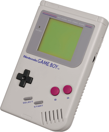
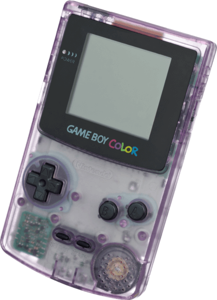
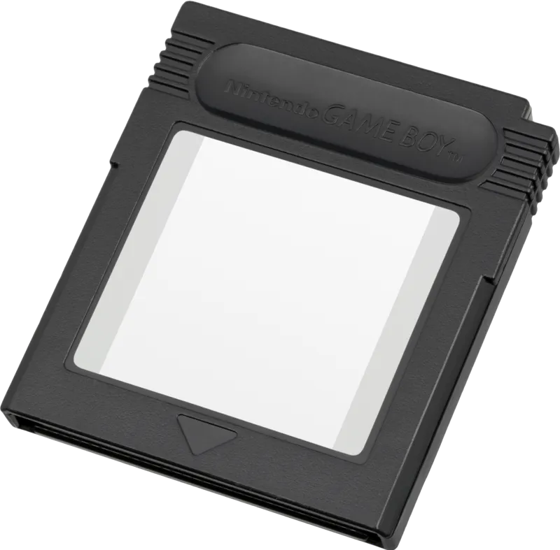
The original Game Boy. Released on 21/04/1989 in Japan, 31/07/1989 in America, and 28/09/1990 in Europe.The next-generation successor called Game Boy Color. Released on 21/10/1998 in Japan, 18/11/1998 in North America, and 23/11/1998 in Europe.
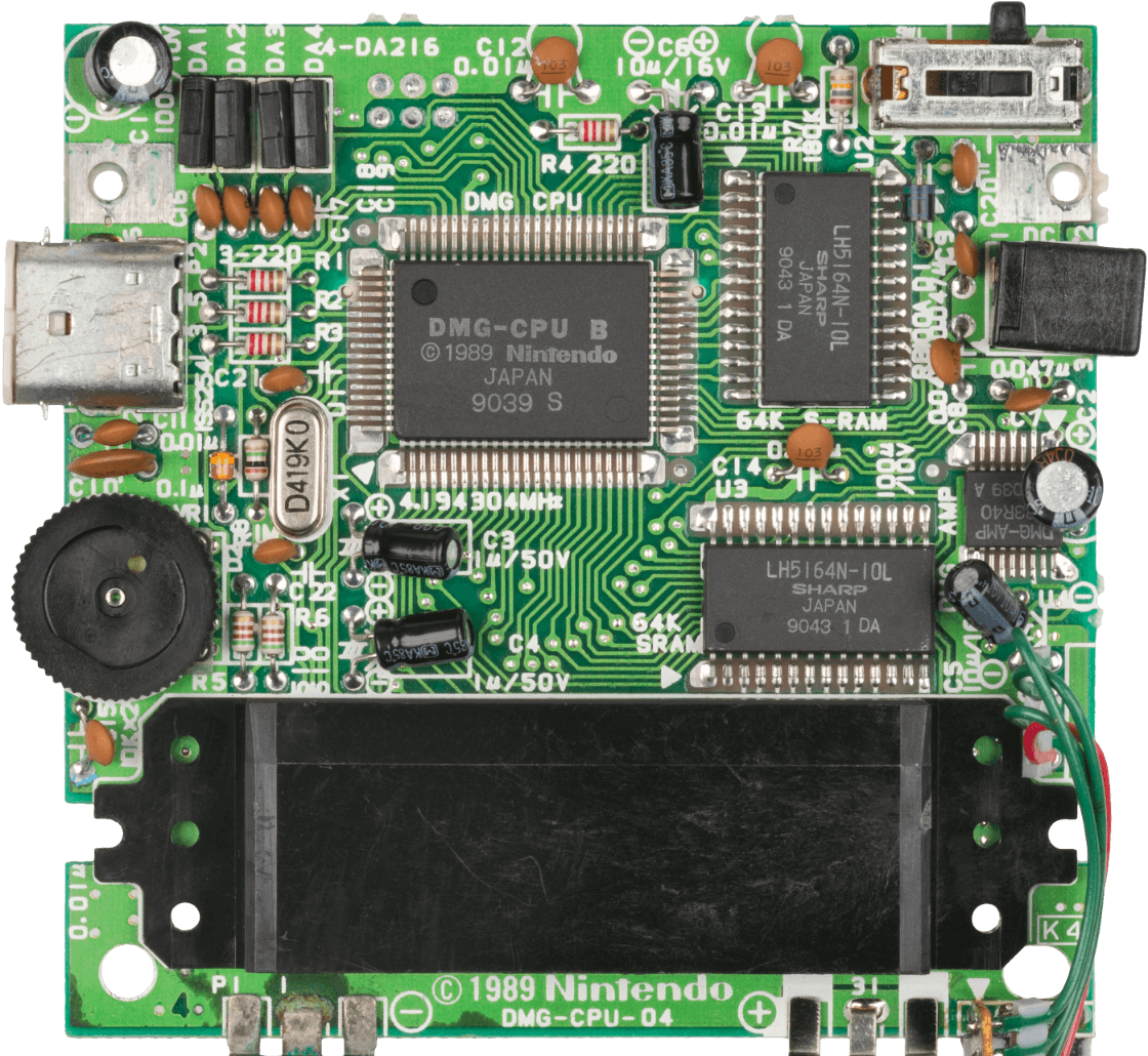
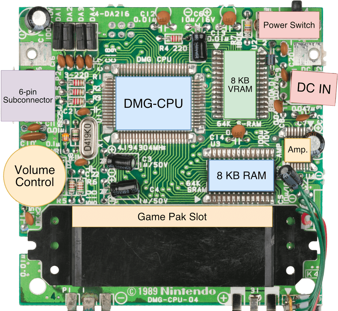
Motherboard Showing revision '04'. Note that 'DMG' is the identifier of the original Game Boy model.Motherboard with important parts labelled
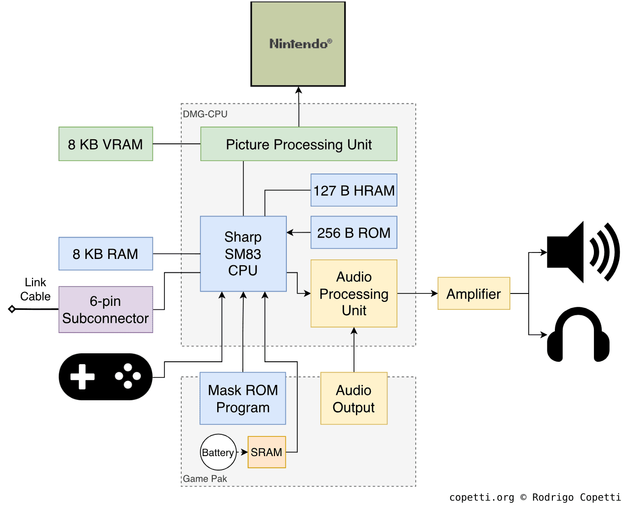
DiagramMain architecture diagram Based on the original Game Boy.
A quick introduction
The Game Boy series can be imagined as a portable version of the Nintendo Entertainment System (NES) with limited power, but you’ll see that it introduced very interesting functionality.
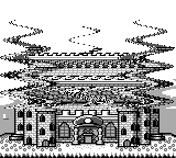
The rainbow analysis
The immense popularity of this console led to a variety of revisions (e.g. Game Boy Pocket, Light, and even adaptations in the form of Super Nintendo cartridges). As a matter of fact, the Game Boy brand spans two generations: within the 4th generation, we find the monochrome Game Boy and its revisions, while the next generation features the Game Boy Color (shipped after the demise of the Virtual Boy).
The good news is that this article covers both ends of the spectrum. So, in the end, you’ll gain a clear understanding of how the Game Boy works and how its technology evolved into the Game Boy Color.
CPU
Instead of placing many off-the-shelf chips on the motherboard, Nintendo opted for a single-chip design to house (and hide) most of the components, including the CPU. This type of design is commonly known as a System-on-Chip (SoC) and, in this case, it was specifically crafted for this console, enabling Nintendo to tailor it to their needs (such as power efficiency, anti-piracy, and extra I/O capabilities). At the same time, the Game Boy’s SoC could not be found in any retail catalogue, meaning competitors had a harder time cloning it.
That being said, the SoC used in the Game Boy is referred to as DMG-CPU or Sharp LR35902[1], and as the name indicates, it was manufactured by Sharp Corporation. This company, along with Ricoh (the NES’ CPU supplier), enjoyed a close relationship with Nintendo.
The CPU core
Inside the DMG-CPU, we find the main processor: a Sharp SM83[2]. This is just a mix of the popular Zilog Z80 (found in the Sega Master System) and the Intel 8080. It runs at ~4.19 MHz, which is faster than the average 1-MHz CPU, but remember clock speeds can be deceiving.
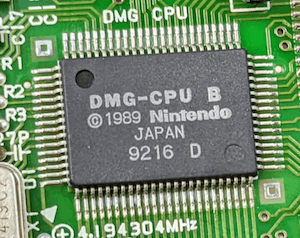
The DMG-CPU chip on my Game Boy’s motherboard.
Now, back when I conducted the analysis of the Master System, I explained the Zilog Z80 is essentially a superset of the Intel 8080. So, what does the SM83 actually retain and omit from those two? [3]
Neither the Z80’s IX and IY registers nor the 8080’s IN or OUT instructions are present. This means that Input/Output (I/O) ports are not available. I’m not certain whether this was a cost-saving measure, but one thing is for sure: components must be completely memory-mapped[4].
Only the Intel 8080’s register set is featured. Consequently, there are only seven general-purpose registers - unlike the Z80 with its 14 (thanks to its additional ‘alternate’ set).
Only portions of the Z80’s extended instruction set are implemented. Specifically, bit-manipulation instructions.
Furthermore, Sharp also added a few new instructions that are not present in either the Z80 or 8080. They optimise certain operations related to the way Nintendo and Sharp arranged the hardware. One example is the new LDH instruction (meaning ‘load high’ [5]), which was strategically designed to access the last 256 bytes of the memory map (where addresses start at $FF00) and, most importantly, fits in one fewer byte (making it slightly faster).
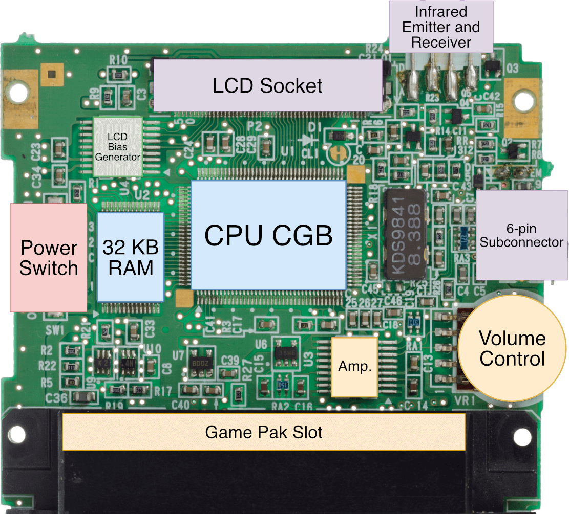
Motherboard of the Game Boy Color [6].The previous picture with important parts labelled.
Nearly a decade later, following the abandonment of the Virtual Boy and its cutting-edge hardware, a humble successor arrived: the Game Boy Color. Inside it, there’s a new SoC named CPU CGB that carries a few additions. However, its SM83 CPU core remains mostly unchanged, one exception is its doubled clock speed (now operating at ~8.38 MHz).
It’s hard to think that, after almost ten years, Nintendo still bundled the same CPU core, but such a decision did come with the following advantages:
Developers could reuse their acquired skills to program the new console.
It reduced costs by eliminating the need to redesign their system for a new architecture.
Backwards compatibility became possible with minimal effort. In fact, Nintendo implemented this by programming two operational modes into CPU CGB:
Normal mode, where the SM83 operates at ~4.19 MHz.
Dual-speed mode, where the SM83 operates at ~8.38 MHz.
However, this came at the expense of adopting outdated technology by late-90s standards. You only have to look at the state of the CPU market to notice the capabilities Nintendo was missing out. Though, to be fair, Nintendo did make an attempt with the Virtual Boy hardware.
Hardware access
The SM83 maintains an 8-bit data bus and a 16-bit address bus, allowing up to 64 KB of memory to be addressed. The memory map is mainly composed of the following regions [7]:
Game Pak (i.e. the game cartridge) space.
Work RAM (WRAM), High RAM (HRAM), and Video RAM (VRAM).
Various I/O (including the joypad, audio, graphics, and LCD).
Interrupt controls.
Now, don’t worry about the unique names - these components are explained throughout this article.
Memory available
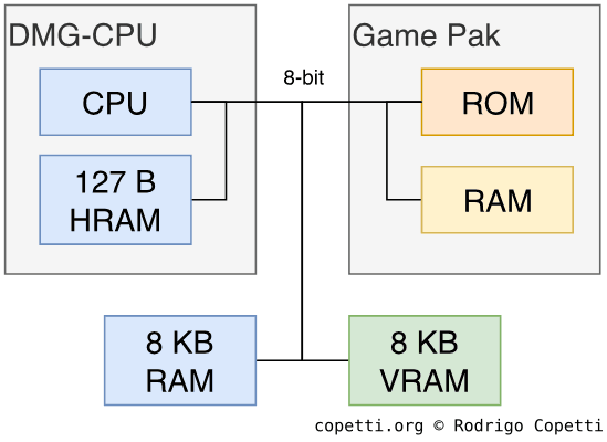
Memory architecture of the DMG (original Game Boy). As you can notice, the PPU arbitrates access to VRAM.
Nintendo fitted 8 KB of RAM onto the motherboard, this is for general purpose use (hence the name Work RAM or ‘WRAM’) [8]. I’m obliged to point out that this is four times the amount included in the NES.
There’s an additional 127 B of RAM housed in the SoC. This is called High RAM (HRAM) and provides a small space for data that can be retrieved faster (via the aforementioned LDH instruction). The idea is very similar to the MOS 6502’s ‘Zero Page’ mode [9], which also optimised performance based on memory location. Apart from this, the High RAM bus is not technically faster than the Work RAM’s, but it is prioritised for the CPU. You’ll see the significance of this in the ‘Graphics’ section, where I discuss Direct Memory Access (DMA).
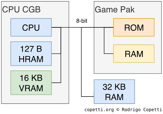
Expanded memory architecture of the CGB (Game Boy Color).
Later on, with the ‘Color’ revision, Nintendo enlarged WRAM to 32 KB. However, since the CPU’s addressing capabilities remained unchanged, it was not possible to connect all the new memory without first overflowing the available address space. To tackle this, Nintendo’s engineers resorted to bank switching within the console itself.
While previously found in NES cartridges, the Game Boy Color applies the principle of bank switching to access the extra 24 KB of WRAM. The trick is simple: the last 4 KB of the original 8 KB space can now be swapped across seven different banks. To make this work, the CPU bundles an extra register (called SVBK) acting as the bank switcher, this is what developers must use to examine the extended memory.
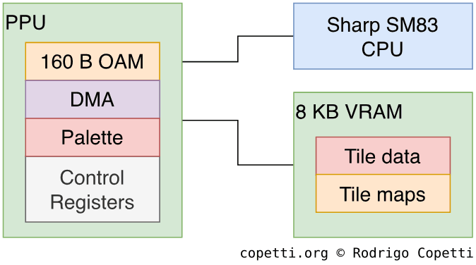
Graphics
In the world of Game Boy graphics, all calculations are done by the CPU, and then the separate Picture Processing Unit (PPU) renders them. This is another component found inside the DMG-CPU SoC, and could be described as an improved version of the predecessor’s graphics chip (which, coincidentally, shares the same name).
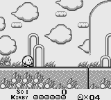
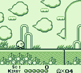
Frame rendered by the PPU.Frame displayed on the original Game Boy’s LCD.Kirby’s Dream Land (1992), sampled from the ‘bgb’ emulator to simulate different screen types.
The picture is displayed on an integrated Liquid-Crystal Display (LCD) with a resolution of 160×144 pixels. In the case of the monochrome Game Boy, the LCD can only reflect 4 shades of grey (white, light grey, dark grey and black). However, due to the use of a green-tinted LCD, the picture will look slightly greenish.
A familiar model
If you’ve read the NES study, you may recall that the PPU was designed to leverage the behaviour of the CRT (especially how its beam worked). This may now seem incompatible when connected to an LCD. Although, the new display still requires to be refreshed. Thus, the new PPU uses this to provide CRT-based effects, similar to those that enabled NES developers to come up with imaginative content.
Additionally, unlike its home console counterpart, the Game Boy is not powered by the alternating current supplied through wall sockets - the very same that varies depending on the country or region. Consequently, the analogue circuitry is not tied to the region’s electrical grid. What I mean to say is, while the NES had to be adapted to 60 Hz and 50 Hz configurations, the Game Boy operates on the same four AA batteries, regardless of geographical location. Therefore, all Game Boys share common CPU clock speeds and a refresh rate of 59.7 Hz - a standard that makes things more pleasant for developers (and, ultimately, users).
Organising the content
Memory architecture of the PPU.
The PPU is exclusively connected to 8 KB of Video RAM (also called ‘VRAM’, though some sources also refer to it as ‘Display RAM’). Those 8 KB contain most of the data the PPU needs to render graphics. The remaining materials are stored within the PPU itself, as they require faster access rates.
The PPU also arbitrates CPU-to-VRAM access, and the game is in charge of populating the different areas with the correct types of data. Moreover, the PPU exposes registers that are used to define how the graphics data is organised. Nevertheless, there are many rules to follow (explained in the following sections).
Constructing the frame
The final frame that you see on the LCD screen is composed of three overlapping layers. Each is designed for a different type of use.
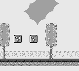
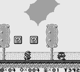
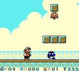
Let’s see how the PPU manages to draw pixels on the screen. For demonstration purposes, Super Mario Land 2 is used as an example.
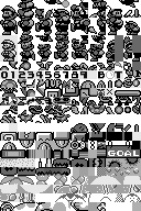
A pattern table with multiple tiles squashed together.A single tile.Tiles found in VRAM.
The PPU uses tiles as a basic ingredient for rendering graphics, specifically, sprites and backgrounds[10].
Tiles are just 8x8-pixel bitmaps. Each occupies 16 bytes and is stored in VRAM, in a region called Tile set or ‘Tile pattern table’. The colour of the pixels comes from one of the four available shades of grey, which is selected through a ‘colour’ palette. The use of palettes also allows colours to be alternated without having to modify the tile set.
The monochrome Game Boys house enough registers to define up to three palettes, yet their use is limited to the type of layer being rendered (explained in the next sections). As previously explained, there are only four colours/shades to choose from, so a single 8-bit register can accommodate a palette of four shades without issue.
Moving on, tiles are grouped into two pattern tables.
To build the picture, tiles are referenced in another type of table known as a Tile map. This data informs the PPU where to render each tile. Two maps are stored to build different layers of the frame.
The following sections explain how tile maps are used to assemble these layers.
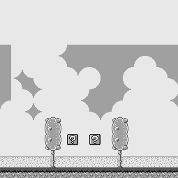
Allocated background map in VRAM.Selected area of the background map. Notice that the selection includes an unpopulated portion at the top. This is intentional and will be later overlapped by the Window layer.Displayed background layer.The background layer rendering process.
The background layer is a 256x256 pixel (32x32 tiles) map containing static tiles. However, remember only 160x144 pixels are visible on the screen. So, the game also decides which portion of the background layer is selected for display. Interestingly, games can also shift the viewable area during gameplay - this is how the scrolling effect is accomplished.
One of the two tile maps is used to construct the background layer. Moreover, only one palette is available for this layer.
Sprites, also known as ‘Objects’, are tiles that can move independently across the screen. They can also overlap one another and appear behind the background; the viewable graphic is determined by a priority attribute.
This layer also has an extra colour available: Transparent. At first, this means sprites can only display three shades of grey instead of four. On the other hand, this layer in particular offers the choice of two dedicated palettes.
The Object Attribute Memory (OAM) is a map stored within the PPU that specifies which tiles are used as sprites, its location makes it faster to access during rendering. For this reason, all sprites are defined in OAM (rather than a tile map within VRAM). Games typically fill this region by calling the OAM Direct Memory Access (DMA) unit located inside the chip; the DMA fetches data from main RAM or game ROM and transfers it to OAM. Now, while DMA is active, the CPU cannot access external memory - hence the importance of taking advantage of High RAM during that period.
In addition to the tile index, each OAM entry contains the following attributes: X-Y position, chosen palette, priority, and flip flags (allowing to mirror the tile vertically and horizontally).
The PPU is limited to rendering up to ten sprites per scan line and up to 40 per frame; overflowing this will result in sprites not being drawn.
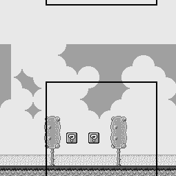
Allocated Window map.Displayed Window map. This is because the game intentionally activates it during the final scan lines. Hence, only the first rows are rendered at the bottom of the screen.The window layer rendering process.
The window layer is a 160x144 pixel map (covering the entire screen) that renders tiles on top of the background and sprites. Having said that, this layer does not scroll.
Only the remaining tile map can be assigned to the window layer, which also shares the same palette.
All in all, this may sound like a silly feature: considering the window lacks transparency and therefore completely obscures all underlying layers, you may wonder ‘what is it useful for?’. Well, in combination with timed raster effects, the window can be used partially across different areas of the screen. Remember the complex and time-sensitive routines NES games went through to display player stats? The window is an answer to that, now automatically handled by the Game Boy’s PPU.
Consequently, games normally use the window layer to draw life counters, scores, and other persistent information.
Once the frame is finished, it’s time to move on to the next one! However, the CPU cannot modify the tables while the PPU is reading from VRAM, so the system provides a set of interrupts triggered when the PPU is idle. You may recall this behaviour from the NES era.
When a single scan line is complete, the Horizontal Blank period starts. This allows developers to fiddle with the part of the frame that has not yet been drawn.
When all scan lines are complete, the Vertical Blank period begins, and a dedicated interrupt is called. The game can then update the graphics for the next frame.
There’s an extra state called OAM search that is initiated at the start of the scan line. At this point, the PPU is determining which sprites will be displayed on that scan line, so the game may update any region except OAM.
Super Mario Land 2: 6 Golden Coins (1992) plays with the X and Y scrolling controls mid-screen.
The inclusion of the window layer and extra interrupts allowed for unique content and effects. For instance, horizontal interrupts made it possible to alter the frame before it was fully drawn. This meant that a different scrolling value could be applied to each line, causing each row of the frame to shift at different rates [11].
This achieved an interesting wobble effect (I’m not sure whether that is its official name, but I find it distinctive enough).
The Color additions
So far, we’ve been focusing on the original Game Boy entry. Let’s now examine the additions of the so-called ‘Color’ model.
Modes of operation
The Legend of Zelda: Link’s Awakening DX (1998). A hybrid Game Boy Color game running in CGB mode.Super Mario Land 2, running in a Game Boy Color. The game executes in DMG mode, but the console applies a colourised palette nonetheless.
The Game Boy Color’s PPU essentially behaves as a superset of the original. Yet, Nintendo wanted Color users to experience enhancements even with monochrome-only games. Thus, to maintain compatibility, the new PPU exhibits two modes of operation:
CGB mode: An extended PPU mode offering all the visual improvements featured in Game Boy Color titles.
DMG mode: A traditional mode with all the extras disabled. Nevertheless, you’ll see in the ‘Operating System’ section that monochrome games are still upgraded with colour palettes.
Organising the (new) content
The CGB motherboard now houses 16 KB of VRAM, which is double the original VRAM amount. Due to the CPU’s addressing limitations, this new arrangement is implemented in the form of two 8 KB banks, with a new register (VBK) acting as a switcher.
Meanwhile, the PPU can access the two banks at the same time. So, at the end of the day, programmers simply need to fill the VRAM banks with the help of VBK, and then specify in the tile map which bank the tile resides in, allowing the PPU to take care of the rest.
That being said, what can you do with the extra VRAM? Many things:
Store twice as many tiles.
Store additional palettes, which also offer a broader colour gamut.
Extend the tile metadata space to encode more effects and reference extra palettes.
The visuals
Thanks to the new PPU, programmers can now define colour palettes with 32,768 colours to choose from.
Firstly, developers must populate a new area called Palette Memory, which stores up to sixteen colour palettes (half for the background and window, and half for sprites), each encoding four colours[12]. Each entry fits in a 16-bit value (2 bytes), though only 15 bits are utilised. Palette Memory is not directly addressable by the CPU; instead, a new register serves as a buffer for writing to this memory (a methodology also found in the Super Nintendo). Overall, this is how coloured games define palettes.
Having said that, background and window tiles can reference any of the eight available palettes. The same applies to sprite tiles, except they are constrained to three-colour palettes, as one entry is still reserved for the ‘transparent’ colour.
The extra space
Moving on, tile sets are now twice as big, enabling programmers to store double the amount of tiles in VRAM. Background and window tile maps have been extended as well, resulting in extra meta-data being encoded. This expands the capabilities of these layers. For instance, background and window tiles can now be flipped horizontally and vertically, saving the need from storing duplicate graphics in VRAM (which, in turn, can be leveraged to render more unique content).
Furthermore, CPU CGB bundles one extra DMA unit, capable of copying data from the Game Pak or WRAM to VRAM. It operates in two modes [13]:
General-purpose DMA: Transfers can happen at any time, with the DMA taking priority over other memory accesses. So, programmers must carefully consider when to use this component (e.g. during or outside scanning) and how much data to copy, as misuse can lead to screen tearing (since VRAM access will be blocked during the transfer).
Horizontal Blank (H-Blank) DMA: Transfers will only occur during H-Blank periods. This avoids screen artefacts, but limits transfers to batches of 16 Bytes, and pauses during LCD scanning.
Once again, this unit offers programmers new opportunities to deliver richer content, as it takes advantage of periods that would otherwise remain idle.
Interestingly, this is one of the few components that remained unchanged across Game Boy revisions. In fact, unlike the CPU, it cannot be accelerated: altering the speed of the oscillators does not improve sound quality, but simply changes the pitch. Instead, more circuitry would be needed to increase the capabilities, and that would also raise the cost.
Functionality
Let’s take a look at the offerings. Each of the four channels is reserved for a single type of waveform:
Pulse 1 channel.Pulse 2 channel.All audio channels.Oscilloscope display of a music score from Pokémon Red/Blue (1996).
Pulse waves have a very distinct beep sound that is mainly used for melody and sound effects.
The APU reserves two channels, each dedicated to a pulse wave. The channels offer four different tones (constructed by varying the pulse width). The first channel features an exclusive sweep control.
Due to the limited number of channels, melodies are often interrupted when sound effects are triggered during gameplay. This is especially noticeable in games like Pokémon Red/Blue when, during a battle, the Pokémon’s cry takes over all music channels.
The mixer outputs stereo sound, meaning channels can be assigned to the left or right side. In other words, the audio subsystem offers panning controls. This is only audible through the headphone line, I’m afraid, as the built-in speaker is mono.
Furthermore, the mixer hardware is also connected to a dedicated pin on the cartridge, allowing the latter to stream an extra channel, provided the cartridge outputs the analogue sound (which is only possible with extra hardware). Nevertheless, no game in the market ended up using this feature, leading to its removal by the time the Game Boy Advance (and its backwards compatible subsystem) arrived.
Operating System
Unlike the NES/Famicom, which booted straight into the game, the Game Boy was designed to always boot from an internal 256-byte ROM, and only then jump to the game code. The boot process is as follows [15]:
After the console is switched on, the CPU starts reading from address 0x0000 (the Game Boy’s ROM location).
RAM and APU are initialised.
The Nintendo logo graphics are copied from the cartridge ROM to Display RAM, and then drawn at the top edge of the screen. If there is no cartridge inserted, the logo will contain garbage tiles. The same may happen if the cartridge is improperly inserted.
The logo is scrolled downwards and the iconic po-ling sound is played.
The game’s Nintendo logo is compared with the one stored in the console’s ROM. Afterwards, a quick checksum is performed on the cartridge’s ROM header to confirm the cartridge is correctly inserted. If either of these checks fail, the console freezes.
The console’s ROM is removed from the memory map.
CPU begins executing the game.
Interestingly enough, the Nintendo logo displayed on the screen is not cleared from VRAM, leaving the opportunity for games to apply some animation and effects to transition to their own logos.
Start of the animation. The logo appears from the top and scrolls down.End of the transition. If the ROM’s checks have passed, the console will proceed to execute the game, otherwise it stays frozen.The original GameBoy’s boot animation.
The revised sequence
The Game Boy Color’s boot screen, the logo doesn’t slide anymore but instead features a rainbow effect.
Once again, in the case of the Game Boy Color, we find drastic changes in the contents of the ROM. For instance, the size of the ROM is now 2 KB[16] and the routines exhibit new behaviour:
The boot sequence now checks whether it’s got a Game Boy-only or Game Boy Color game inserted, and then sets the corresponding registers to activate DMG or CGB mode. To do this, the boot code examines specific game metadata (within the cartridge’s ROM) that is structured differently for CGB games.
If a DMG game is inserted, the boot program also fills Palette RAM with calculated palettes. These are based on a simple yet clever algorithm that also relies on the game’s metadata. This is what gives monochrome games a coloured appearance when running on the next-generation console.
At this stage, the user may press a button combination to alter the boot code’s palette of choice.
For some reason, the Nintendo logo is copied to HRAM as well, and the checksum stage will only check the first half of the logo in HRAM.
Games
One of the main constraints of 70s-80s consumer hardware was its programming limitations: while promising, high-level languages like C or Pascal were not yet ready for performance-critical applications, as compilers lacked maturity and games had to squeeze as much performance as possible. As a result, Game Boy games were mainly written in assembly language.
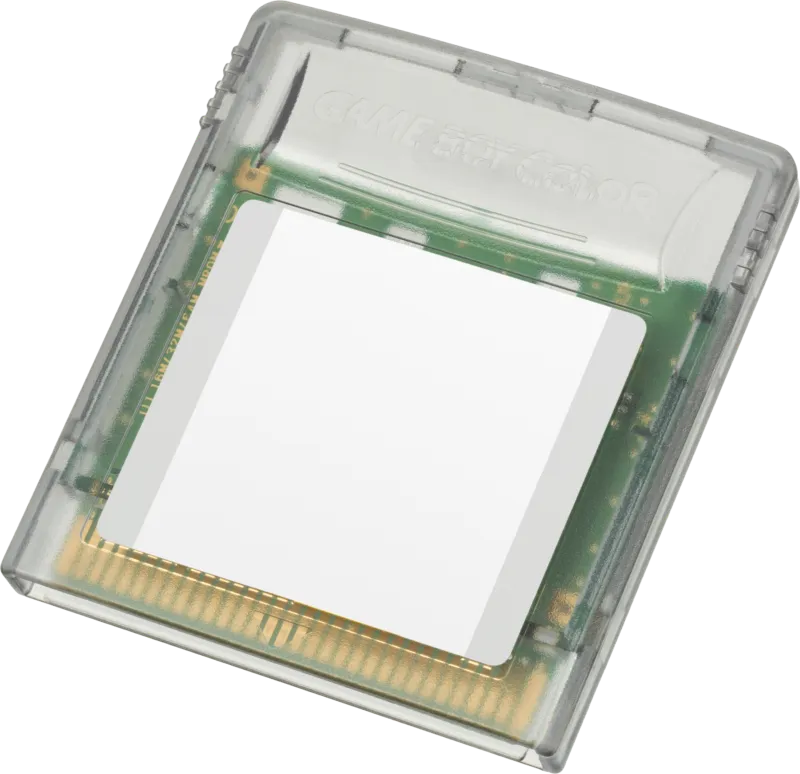
Apart from this, commercial games were distributed in the form of Game Paks, which were cartridges designed by Nintendo for the Game Boy series. In terms of storage options, games had a maximum size of 32 KB, owing to the limited address space available. However, with the help of a Memory Bank Controller (mapper), games could reach bigger sizes. The largest Game Pak found in the market featured a 1 MB ROM (or 8 MB, in the case of the Game Boy Color).
Finally, some Game Paks also included a real-time clock and/or extra Static RAM (SRAM), along with an external battery to hold saves.
Modernised cartridges
Black design [18], denoting ‘Game Boy Color enhanced’.Translucent design [19], denoting ‘Game Boy Color exclusive’.Color-era revisions of the Game Pak.
With the addition of an extra mode of operation (supported by the Game Boy Color), Nintendo categorised three different types of Game Boy games:
Game Boy: Fully compatible with all Game Boy models. It always runs in DMG mode.
Game Boy Color enhanced: A hybrid that adapts itself based on the host console. While fully compatible with the monochrome model, it is visually enhanced when running in CGB mode on the Game Boy Color. However, the overall functionality remains constrained to ensure compatibility with the very-first Game Boy.
Game Boy Color exclusive: Only compatible with the Game Boy Color, but optimised to take full advantage of its hardware.
The three types were also given official colours to help differentiate them. Yet, some games like Pokémon and Donkey Kong featured alternative designs.
External communications
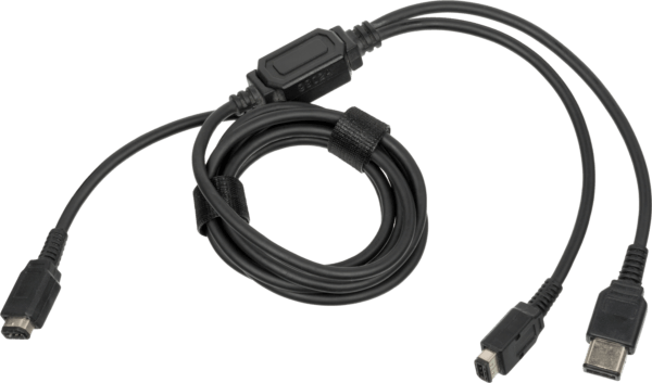
For the first time, games could communicate with external hardware using a Game Boy Link cable, enabling multiplayer functionality and the use of accessories. The Link cable connected to the 6-pin subconnector on the console, with the other end attached to another Game Boy or accessory.
The interface relies on the Serial Peripheral Interface (SPI) protocol, where one Game Boy designates itself as the master (driving the clock signal) and the other becomes the slave. During each transfer, both master and slave exchange an 8-bit packet (1 byte) [20].
The Game Boy Link cable, with alternative plugs to support multiple variants of the console [21]. Since the release of the original Game Boy, subsequent revisions miniaturised the socket while keeping the same number of pins.
The original Game Boy transferred information at 8 Kbit/second (1 KB/sec), while the Color variant could drive a higher clock speed, reaching up to 512 Kbit/second (64 KB/sec). This was known as ‘high speed’ mode.
At one point, Nintendo also shipped a ‘4-Player Adapter’ to allow up to four Game Boys to exchange data simultaneously. The base protocol (SPI) remained the same, but the adapter, now acting as the master, implemented an extra layer of communication that games had to follow to broadcast data to the other consoles [22].
Wireless methods
The Color model also bundled an infrared emitter and receiver (made of an LED and a phototransistor, respectively) [23]. This made it possible to exchange data wirelessly between Game Boy Colors, as seen in titles such as Pokémon Gold and similar. However, you will find that the system didn’t implement a communication protocol - only a single register (RP) that encoded the IR sensor’s action (emit or receive), the bit (0 or 1) being transferred, and the last bit received. Nevertheless, to alleviate things for developers, Nintendo did provide a reference implementation in the official Game Boy Developer Manual [24].
Anti-piracy
As you’ve seen in the ‘Operating System’ section, the console never runs a game straight away; it first performs a series of checks that prevent the execution of unauthorised cartridges and also make sure the cartridge is correctly inserted.
To be able to pass these checks, games had to include a copy of Nintendo’s logo (in the form of tiles) within the ROM header [25]. This way, Nintendo could make use of copyright and trademark laws to control distribution. Pretty clever, huh?
Conversely, Sega v. Accolade later awarded companies the right to use copyrighted logos for this kind of requirement, as it was deemed fair use.
That being said, additional anti-piracy measures could be implemented inside games. Examples included checking the SRAM size (as it’s typically larger in bootlegs) and checksumming the ROM at random points during gameplay (to spot modifications in the game’s code).
That’s all folks
Contributing
This article is part of the Architecture of Consoles series. If you found it interesting then please consider donating. Your contribution will be used to fund the purchase of tools and resources that will help me to improve the quality of existing articles and upcoming ones.
You can also buy the book editions in English. I treat profits as donations.
A list of desirable tools and latest acquisitions for this article are tracked in here:
### Interesting hardware to get (ordered by priority)

- An original Gameboy (~£30 ?)
- A Dev cartridge (couldn't find one, yet)
This work is licensed under a Creative Commons Attribution 4.0 International License. You may use it for your work at no cost, even for commercial purposes. But you have to respect the license and reference the article properly. Please take a look at the following guidelines and permissions:
Article information and referencing
For any referencing style, you can use the following information:
Title of article: Game Boy / Color Architecture - A Practical Analysis
@misc{copetti-gameboy,url={https://www.copetti.org/writings/consoles/game-boy/},title={Game Boy / Color Architecture - A Practical Analysis},author={Rodrigo Copetti},year={2019}}
or a IEEE style citation:
[1]R. Copetti, "Game Boy / Color Architecture - A Practical Analysis", Copetti.org, 2019. [Online]. Available: https://www.copetti.org/writings/consoles/game-boy/. [Accessed: day- month- year].
Special use in multimedia (Youtube, Twitch, etc)
I only ask that you at least state the author’s name, the title of the article and the URL of the article, using any style of choice.
You don’t have to include all the information in the same place if it’s not feasible. For instance, if you use the article’s imagery in a Youtube video, you may state either the author’s name or URL of the article at the bottom of the image, and then include the complete reference in the video description. In other words, for any resource used from this website, let your viewers know where it originates from.
This is a very nice example because the channel shows this website directly and their viewers know where to find it. In fact, I was so impressed with their content and commentary that I gave them an interview 🙂.
Appreciated additions
If this article has significantly contributed to your work, I would appreciate it if you could dedicate an acknowledgement section, just like I do with the people and communities that helped me.
This is of course optional and beyond the requirements of the CC license, but I think it’s a nice detail that makes us, the random authors on the net, feel part of something bigger.
Third-party publishing
If you are interested in publishing this article on a third-party website, please get in touch.
If you have translated an article and wish to publish it on a third-party website, I tend to be open about it, but please contact me first.
It’s always nice to keep a record of changes. For a complete report, you can check the commit log. Alternatively, here’s a simplified list:
### 2025-10-17
- Overall improvements to prepare for a book release.
### 2024-01-01
- Various corrections and extensions (see https://github.com/flipacholas/Architecture-of-consoles/pull/245), thanks @ISSOtm- Updated bibliography (see https://github.com/flipacholas/Architecture-of-consoles/issues/244), thanks @ISSOtm### 2023-12-26
- Included the Game Boy Color (the missing puzzle piece) in the analysis.
- Thanks @Sono from #gbdev for clarifying how VRAM banking works (from the CPU and PPU perspective).
- Added max game ROM size for GBC games, thanks @Dwedit.
### 2021-05-16
- Renamed CPU from 'LR35902' to 'SM83', as 'Game Boy: Complete Technical Reference' by Joonas Javanainen (gekkio) suggests it's a more accurate name for the CPU itself (distinguished from the SoC)
- Improved 'Sources' structure
### 2020-11-28
- Corrected wave channel info (see https://github.com/flipacholas/Architecture-of-consoles/issues/15), thanks @lotrbuilders### 2020-10-23
- Overall revamp
### 2020-10-21
- Updated diagram and marked motherboard photo
### 2019-09-17
- Added a quick introduction
### 2019-07-22
- Improved Anti-Piracy content
### 2019-05-19
- Extended CPU section
### 2019-02-21
- Ready for publication
Rodrigo Copetti
I hope you have enjoyed this article! If you want to know more about the author tap here and if you would like to support him tap here instead