This article is also published in many bookstores for the benefit of offline readers. The eBooks are DRM-free, while the printed editions compile multiple articles and feature original photography at full resolution.
You can find printed compilations here, and individual eBooks at Amazon Kindle, Apple Books, Kobo and other stores. The proceeds support the improvement of current articles and the development of new ones.
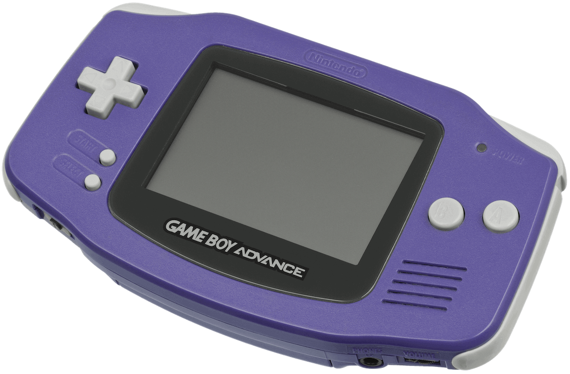
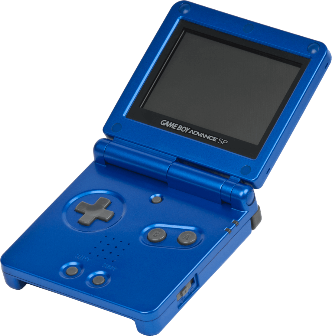
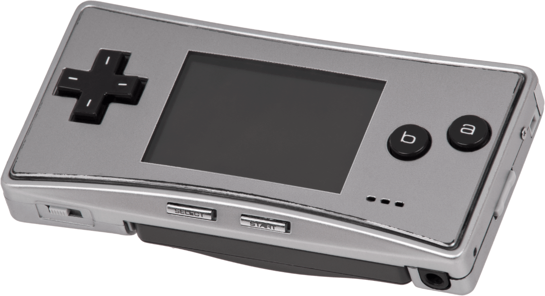
The original Game Boy Advance. Released on 21/03/2001 in Japan, 11/06/2001 in America, and 22/06/2001 in Europe.The Game Boy Advance SP. Released on 14/02/2003 in Japan, 23/03/2003 in America, and 28/03/2003 in Europe.The Game Boy Micro. Released on 13/09/2005 in Japan, 19/09/2005 in America, and 04/11/2005 in Europe.
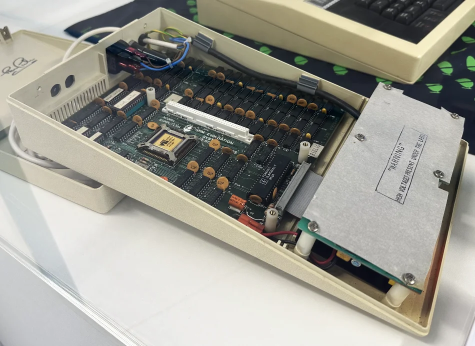
Motherboard Showing the original model, revision '03'. 'AGB' is the codename of the Game Boy Advance. The audio amplifier is on the back.Motherboard with important parts labelled
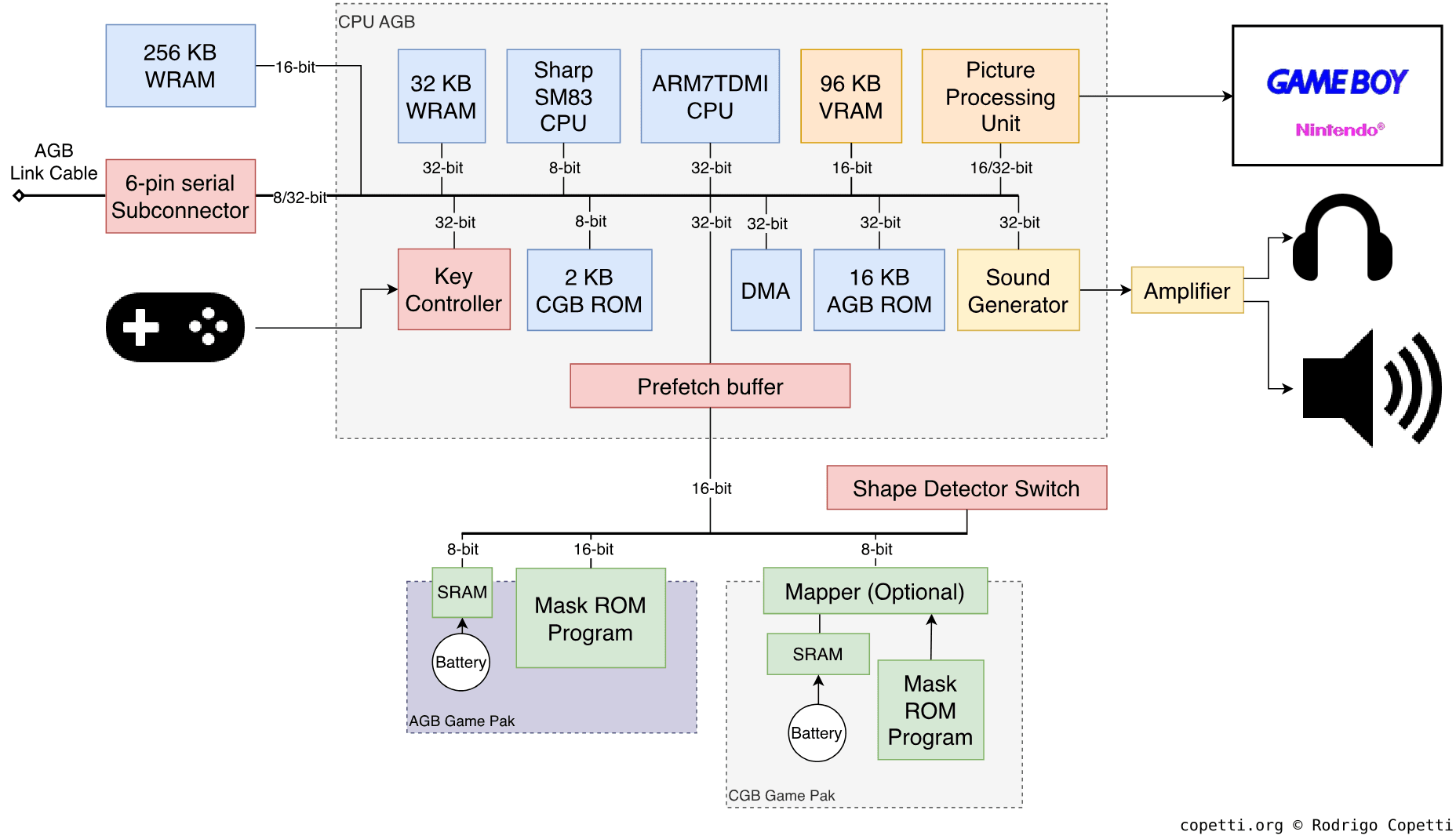
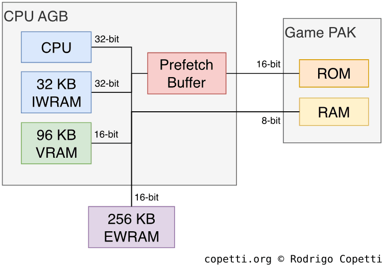
DiagramMain architecture diagram Each data bus is labelled with its width. The layout shown of the AGB Game Pak doesn't include a mapper (as the new CPU is able to address significantly more memory), although games with a large ROM may still bundle one.
A quick introduction
The internal design of the Game Boy Advance is quite impressive for a portable console that runs on two AA batteries.
This console will carry on using Nintendo’s signature sprite engine. Additionally, it will introduce a relatively new CPU from a British company that will surge in popularity in the years to come.
Models and variants
The Game Boy Advance, as a brand, comprises four variants. To quickly summarise:
The original model debuted the new architecture. It was a radical departure from the Game Boy series, both in terms of design and internals, while also managing to provide backwards compatibility.
The ‘Special’ or SP variant offered external quality-of-life improvements (a rechargeable battery, clamshell design, and an illuminated screen).
The Game Boy Micro is a miniaturised version with similar improvements, though this time at the expense of backwards compatibility.
The Game Boy Player is a modularised version that attaches below the GameCube using the Hi-Speed port. It is operated through the GameCube and, thanks to the fact it houses most of the internals of the original console, it offers native and backwards compatibility. However, its distinct shape makes it physically and ergonomically incompatible with many accessories.
I have to say, Game Boy backwards compatibility is an intriguing topic, so I have dedicated a few paragraphs at the end of the CPU section.
CPU
Most of the building blocks of this console are combined into a single package called CPU AGB. This contains two entirely different CPUs:
A Sharp SM83 running at either 8.4 or 4.2 MHz. If it isn’t the same CPU found on the Game Boy! It’s effectively used to run Game Boy (DMG) and Game Boy Color (CGB) titles. My previous article provides an overview of the predecessor.
An ARM7TDMI running at 16.78 MHz: This is the new processor we will focus on, it most certainly runs Game Boy Advance games.
Note that both CPUs will never run at the same time or do any fancy co-processing. The only reason for including the very old Sharp is for backwards compatibility.
With that in mind, let’s dive into the ARM chip. However, since this is the first ARM CPU discussed in this series, let me start with the background history, I promise it will be worth it!
The Cambridge miracle
The story about the origins of the ARM CPU and its subsequent rise to fame is riveting. Here we find a combination of public investment, exponential growth, ill-fated decisions, and long-distance partnerships.
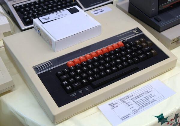
The BBC Micro (1981) with a box of 5¼ disks on top [1], the first disk features the game Elite (1984).The ARM Evaluation Board (1986), a ‘Tube’ module carrying an ARM1 CPU. I found it at The Centre for Computing History (Cambridge, UK).The predecessors of the first commercial ARM CPU, the ARM2.
The late 70s were a tumultuous time for the United Kingdom populace. The interventionist economy once built under post-war ideals had reached its course, and the pendulum soon swung towards free-market reforms. Amid this storm, Cambridge-based ventures such as Acorn Computers, along with Sinclair and the like, were selling computer kits to laboratories and hobbyists. Similarly to American and Japanese enterprises, Acorn’s computers relied on the 6502 CPU and a proprietary BASIC dialect.
Entering the 80s, ministerial interests within the new British government led to the creation of a project aimed at uplifting computer literacy in schools [2]. Thanks to Acorn’s upcoming ‘Proton’ home computer, the company was awarded the contract to build an affordable computer that would realise the government’s vision. The result was the BBC Micro (nicknamed the Beeb), which enjoyed significant success among schools, teachers, and pupils. Inside the Micro, Acorn incorporated an avant-garde ‘Tube’ interface that could expand the computer with a second processor. This paved the way for Acorn’s next big investment.
During the development of their next product, this time enterprise-focused, Acorn did not find a suitable CPU to succeed the 6502. Pressure to innovate in the face of Japanese and American competition, coupled with unfortunate planning, placed Acorn in a troubled financial state. Thus, a new division in Acorn was tasked to produce a compelling CPU. To work around Acorn’s recent constraints, the CPU team based their architecture on the teachings of a research paper called The Case for the Reduced Instruction Set Computer[3] and its prototype, the RISC CPU[4]. Finally, in 1985, Acorn delivered the ARM1 CPU as a Tube module for the BBC Micro, although it was marketed solely for R&D purposes. It won’t be until 1987, with the introduction of the first Acorn Archimedes computer, that ARM chips (by then, the ARM2 CPU) would take a central role.
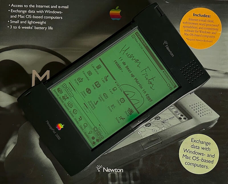
A late Newton model… after a few minutes playing with it.
During the commercialisation of the Acorn Archimedes, Apple became captivated by Acorn’s energy-efficient CPUs, but the American company was still unconvinced that Acorn’s latest ARM3 was suitable for Apple’s new pet project, the Newton. However, rather than walking away (after all, Acorn was a competitor), both explored the possibility of evolving the ARM3 to meet Apple’s requirements [5], namely flexible clock frequency, an integrated Memory Management Unit (MMU), and complete 32-bit addressing.
This collaboration soon turned into a partnership in which Acorn, Apple, and VLSI (ARM’s chip manufacturer) set up a new company solely focused on developing ARM CPUs. Apple provided the investment (obtaining a 43% stake), Acorn shared its staff, and VLSI took care of manufacturing. In 1990, Advanced RISC Machines (ARM) Ltd came into existence, with Robin Saxby appointed as executive chairman.
Years after, Apple finally shipped the Newton MessagePad, powered by an ARM610 - one of the next-generation ARM chips shaped by Apple’s input. Meanwhile, Acorn also released the RiscPC using the new CPUs.
Now, while Acorn and Apple lingered on the computer/handheld market, ARM devised a radical business model. Keeping away from manufacturing, Saxby’s vision centred on licensing ARM’s intellectual property, in the form of CPU designs and its instruction set[6]. This granted ARM with clients beyond the computer realm, such as Texas Instruments [7], which later connected the company to the emerging mobile market (culminating in the Nokia 6110) and set-top boxes. The follow-up years would see ARM’s technology being bundled in billions of mobile devices [8].
Back in Japan, and thanks to the Game Boy analysis, we have learnt that Nintendo’s hardware strategy for portable systems favours a System On a Chip (SoC) model. This has allowed the company to obfuscate affordable off-the-shelf technology and combine it with in-house developments. In doing so, the new console could be unique and competitive. Fortunately, ARM’s licensing model fitted just right for those needs.
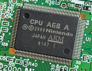
The CPU AGB chip, housing the ARM7TDMI CPU (among many other components).
Both companies had been in discussions since 1994 (a year before the Virtual Boy‘s launch), likely as part of ’Project Atlantis’, during which Nintendo considered the ARM710 [9]. However, nothing materialised until many years later [10], and the reason was simple: the Japanese found ARM’s code density and the need for 32 data wires unfeasible (something the Virtual Boy’s CPU had already managed to escape). Nevertheless, ARM’s new CPU designer - Dave Jaggar - quickly answered with the ARM7TDMI, a new design that focused on maximising performance under power and storage constraints. This marked a turning point for ARM, as this new product not only pleased Nintendo, but also got the attention of Texas Instruments, Nokia, and other competitors in the cellphone arena.
Unsurprisingly, when Nintendo started working on the successor of the Game Boy Color, their CPU pick became the ARM7TDMI.
The ARM7TDMI
Let’s now examine what this chip has to offer.
Commanding the CPU
To begin with, the ARM7TDMI implements the ARMv4 instruction set, the successor of the ARMv3. This implies:
A RISC-based design: As explained before, ARM CPUs have been influenced by a paper from the University of California, Berkeley called ‘The Case for the Reduced Instruction Set Computer’ [11]. Its research outlines a series of guidelines for scalable processor design and advocates the use of a load-store architecture, fixed instruction size, and a large register file. Many of these traits were absent from the crowded CPU market at the time (i.e. the Intel 8086, MOS 6502, Zilog Z80, and the Motorola 68000), but they would influence the design of new CPU lines throughout the 80s and 90s.
Conditional execution: A peculiar feature of the ARM ISA. Essentially, almost every instruction embeds a condition that states whether it should be executed. Typically, other CPUs follow the ‘compare and jump’ process (also called ‘branching’) to control which instructions the CPU must execute. By contrast, ARM programmers may insert the condition in the instruction itself. This is possible due to the first four bits of ARM’s opcodes are reserved for a condition (i.e. equal, not equal, etc). All in all, this reduces the complexity of ARM code, as conditional execution provides a cleaner design for routines, unlike branching and subroutine splitting. Additionally, this also serves as a workaround for control hazards (explained in more detail later).
A flexible second operand, also known as ‘Operand2’ [12]. Typically, operations are made of two operands (like add 2 and 2). However, ARM instructions also allows embedding an extra shift operation into the second operand. For example, you can compute shift 2 by four bits and then add it to 2 in a single instruction.
Bit shifting is also a cheap shortcut to perform division or multiplication with powers of 2, which leads to many optimisation techniques.
32-bit and 64-bit multiplication instructions: An addition in ARMv4. Furthermore, 64-bit operations output the result in two registers.
The package
Now that we know how developers talk to this chip, let’s check what’s inside the silicon.
In terms of circuitry, the ARM7TDMI is a cut-down version of the ARM710 with interesting additions. The core includes [13][14]:
16 general-purpose 32-bit registers: While it’s a big step compared to the seven 8-bit registers of the SM83/Game Boy, it represents a compromise on the RISC guidelines, which stipulate thirty-two 32-bit registers. This is because ARM favoured maintaining a small silicon footprint [15].
32-bit data bus and ALU: Meaning it can move and operate 32-bit values without consuming extra cycles.
Clean 32-bit addressing: This is part of Apple’s input. The first three ARM CPUs employed 26-bit memory addresses to optimise performance (allowing to store the Program Counter and Status Register in a single 32-bit word) in exchange for memory addressability (only up to 64 MB of memory could be accessed). The follow-up ARM6 series (with its ARMv3 ISA) introduced 32-bit addressing logic, but kept a backwards-compatible mode for legacy code. Now, the ARM7TDMI (being mobile-focused) scrapped the 26-bit mode and only houses logic for 32-bit addresses, thereby reducing the amount of silicon needed.
No Memory Management Unit (MMU): Ever since the ARM1, ARM provided an MMU solution. First as the ‘MEMC’ co-processor, and then integrated with the ARM610. Now, the ARM7TDMI seems to be the only one in its series to provide none, potentially due to the lack of interest (as early mobile devices didn’t require sophisticated virtual memory).
No cache: Another cost-saving measure in this chip, as earlier ARM chips bundled some cache.
Finally, all of this can operate with a 3 Volt power supply [16]. This is an evident step towards mobile computing, as earlier cores required a 5 V supply.
Since its first iteration, ARM has implemented a three-stage pipeline to run code. In other words, the execution of instructions is divided into three steps or stages. The CPU will fetch, decode and execute up to three instructions concurrently. This enables maximum use of the CPU’s resources (which reduces idle silicon) while also increasing the number of instructions executed per unit of time.
Like two closely relatedcontemporaries, ARM CPUs are susceptible to data hazards. Nevertheless, neither the programmer nor the compiler will notice them, as, in this case, the CPU automatically stalls the pipeline when necessary.
Control hazards are also present, but ARM tackled them with an efficient approach called conditional annulment: whenever a branch instruction reaches the second stage (Decode), the CPU evaluates the branch condition [17]. Based on the result, if the branch is to be taken, the CPU automatically nullifies the follow-up instruction (turning it into a filler). Now, this may look inefficient when compared to MIPS’ approach (as a MIPS compiler can insert useful instructions, not just fillers). Hence, apart from branching, ARM provides conditional execution. The latter turns this pipeline design into an advantage, since ARM can decode an instruction and calculate its embedded condition at the same stage. Thus, in this case, no fillers are added. This is why conditional execution is preferred over branching when programming for ARM CPUs [18].
One of the drawbacks of load-store architectures led to ARM’s code being very sparse. Competitors like x86 could perform the same tasks using smaller amounts of code, requiring less storage. Consequently, when Nintendo took a look at ARM’s latest design, the ARM7, they weren’t pleased with it. The size of ARM’s instructions meant that hypothetical gadgets comprised of 16-bit buses with limited memory and storage - all to save cost and energy - would make the CPU inefficient and bottlenecked. Luckily, Dave Jaggar had just finished designing the ARM7 and wouldn’t give up yet. During his commute after meeting Nintendo, he came up with a solution: The Thumb instruction set[19].
Thumb is a separate instruction set that operates as an alternative mode within the CPU. It is comprised of a subset of the ARM instruction set, with instructions encoded into 16-bit words (as opposed to 32-bit) [20]. Being 16-bit, Thumb instructions require half the bus width and occupy half the memory. To achieve this, it compromises in the following ways:
Thumb doesn’t offer conditional execution, relying on branching instead.
Its data-processing opcodes adopt a two-address format (e.g. add R1 to R3), rather than a three-address format (e.g. add R1 and R2 and store the result in R3).
It only has access to the lower half of the register file. Thus, only eight general-purpose registers are available.
All in all, since Thumb instructions offer only a functional subset of ARM, developers may have to write more instructions to achieve the same effect. In practice, Thumb uses 70% of the space of ARM code. For 16-bit wide memory, Thumb runs faster than ARM. If required, ARM and Thumb instructions can be mixed in the same program (called interworking) so developers can choose when and where to use each mode.
The ARM7TDMI is, at its essence, an ARMv3-compliant core with extras. The latter is referenced in its name (TDMI), meaning:
T → Thumb: The inclusion of the Thumb instruction set.
D → Debug Extensions: Provide debugging capabilities using the Joint Test Action Group (JTAG) interface.
M → Enhanced Multiplier: Previous ARM cores required multiple cycles to compute full 32-bit multiplications, this enhancement reduces it to just a few.
I → EmbeddedICE macrocell: Enables hardware breakpoints, watchpoints, and allows the system to be halted while debugging code. This facilitates the development of programs for this CPU.
Overall, this made the ARM7TDMI an attractive solution for mobile and embedded devices.
The inclusion of Thumb in particular had a strong influence on the final design of the Game Boy Advance. Nintendo mixed 16-bit and 32-bit buses between its different modules to reduce costs, all while providing programmers with the necessary resources to optimise their code.
Memory architecture of this system.
The Game Boy Advance’s usable memory is distributed across the following locations (ordered from fastest to slowest) [21]:
IWRAM (Internal WRAM), 32-bit with 32 KB: Useful for storing ARM instructions.
VRAM (Video RAM), 16-bit with 96 KB: While this block is dedicated to graphics data (further explained in the next section), it also appears in the CPU’s memory map. So, programmers can store other data here if IWRAM is not enough.
EWRAM (External WRAM), 16-bit with 256 KB: A separate chip next to CPU AGB. It’s optimal for storing Thumb-only instructions and small data chunks. On the other hand, the chip can be up to six times slower to access compared with IWRAM.
Game PAK ROM, 16-bit with variable size: This is the place where the cartridge ROM is accessed. While one of the slowest sources, it is mirrored in the memory map to offer different access speeds. Additionally, Nintendo fitted a Prefetch Buffer that interfaces the cartridge to reduce stalling and compensate for the lack of CPU cache. This component independently caches continuous addresses when the CPU is not accessing the cartridge. It can hold up to eight 16-bit words.
In practice, however, the CPU rarely lets the Prefetch Buffer do its job. Since, by default, the CPU continuously fetches instructions from the cartridge to maintain execution [22]. This is why IWRAM and EWRAM are so critical.
Game PAK RAM, 8-bit with variable size: Used to access cartridge RAM (SRAM or Flash Memory).
This is strictly an 8-bit bus (the CPU will see ‘garbage’ in the unused bits).
In conclusion, even though this console was marketed as a 32-bit system, the majority of its memory is only accessible through a 16-bit bus, meaning games mostly use the Thumb instruction set to avoid spending two cycles per instruction fetch. Only in very exceptional circumstances (e.g. when using instructions not found on Thumb or when reading from IWRAM) programmers will benefit from the ARM instruction set.
Becoming a Game Boy Color
Apart from the inclusion of GBC hardware (e.g. the Sharp SM83 CPU, original BIOS, audio and video modes, and a compatible cartridge slot), there are two further functions required to make backwards compatibility work.
From the hardware side, the console relies on an electrical switch to detect if a Game Boy or Game Boy Color cartridge is inserted [23]. A shape detector in the cartridge slot effectively identifies the type of cartridge and allows the ARM7 CPU to read its state and act accordingly. Furthermore, the voltage supply, along with the joypad, cartridge, and WRAM buses are physically redirected depending on the state of the switch.
From the software side, there is a special 16-bit register called REG_DISPCNT which can alter many properties of the display, but one of its bits sets the console to ‘GBC mode’ [24]. This prompts the system to put the SM83 CPU in charge and bootstrap the GBC BIOS. There’s one restriction, however: setting REG_DISPCNT to GBC mode only works if the system is currently booting from the GBA BIOS, as it checks the value of the program counter (the PC register).
An interesting aspect reported in the Gbdev Wiki and GBATek is that all Game Boy Advance variants are technically capable of executing Game Boy code[25][26]. This includes the Game Boy Micro, which lacks the legacy cartridge slot. This is because all variants bundled the same SoC and they don’t strictly need the shape detector to enter GB mode. Additionally, by fiddling with other registers, the GB’s verification routines can be bypassed. However, in the absence of a GB cartridge, the GB game must somehow reside in VRAM (since the CPU will be reading zeroes until reaching VRAM) and the joypad becomes unusable (as the shape detector must be switched to redirect the bus to the SM83) [27].
Graphics
Before we begin, you’ll find the graphics capabilities to be a blend of Super Nintendo and Game Boy elements. In fact, the new graphics core is still called PPU. Thus, I recommend reading those articles first, as I will be revisiting many previously explained concepts.
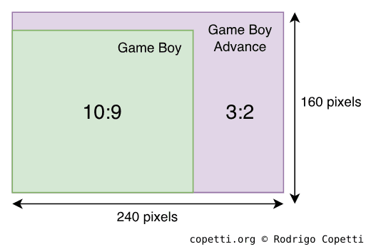
Comparison of screen resolution and aspect ratio between the Game Boy and Game Boy Advance series.
Compared to previous Game Boys, we now have an LCD screen with a richer colour gamut, capable of displaying up to 32,768 colours (15-bit). It features a resolution of 240 x 160 pixels (giving games a ‘wide-screen’ look) and a refresh rate of ~60 Hz. I wonder if the new aspect ratio was directed towards benefiting platform games.
Organising the content
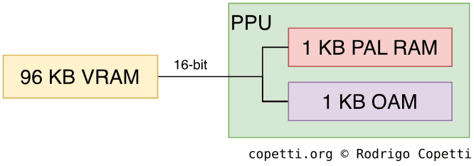
Memory architecture of the PPU.
Graphics data is distributed across these memory regions:
96 KB 16-bit VRAM (Video RAM): 64 KB store backgrounds and 32 KB store sprites.
1 KB 32-bit OAM (Object Attribute Memory): Houses up to 128 sprite entries (not the graphics, just the indices and attributes). As noted by its wide bus, OAM is exclusively optimised for fast access.
1 KB 16-bit PAL RAM (Palette RAM): Holds two big palettes, one for backgrounds and one for sprites. Each palette contains 256 entries of 15-bit colours each, where colour 0 means transparent.
Constructing the frame
If you’ve read the previous articles, you’ll find the GBA familiar, although there is additional functionality that may surprise you. Regardless, the fact the new system operates on just two AA batteries makes this study even more enthralling.
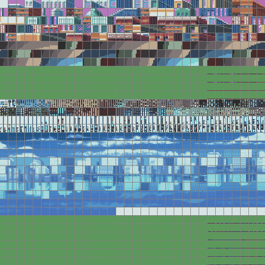
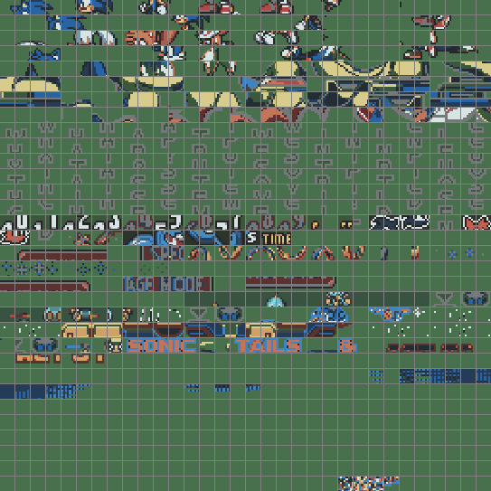
Now I’m going to borrow the graphics of Sega’s Sonic Advance 3 to show how a frame is composed.
These two blocks are made of 4 bpp tiles.You may notice some weird vertical patterns in here, these are not graphics but ‘Tile Maps’ (explained in the next section).These two blocks are reserved for sprites.Pairs of charblocks found in VRAM.
GBA’s tiles are still 8 x 8 pixel bitmaps, but they can now use either 16 colours (4 bpp) or 256 colours (8 bpp). 4 bpp tiles consume 32 bytes, while 8 bpp ones take 64 bytes.
Tiles can be stored anywhere in VRAM. However, the PPU expects them to be grouped into charblocks - continuous regions of 16 KB. Each charblock is reserved for a specific type of layer (either background or sprites), and programmers decide where each charblock begins. This can result in some overlapping, which in turn enables two charblocks to share the same tiles.
Due to the size of a charblock, up to 256 8 bpp tiles or 512 4 bpp tiles can be stored per block. Overall, up to six charblocks can be allocated, which combined require 96 KB of memory - the exact amount of VRAM this console has.
Finally, only four charblocks can be used for backgrounds, while two may be used for sprites.
Background Layer 0 (BG0).Background Layer 2 (BG2).Background Layer 3 (BG3). This particular layer will be shifted horizontally at certain scan-lines to simulate water effects.Static background layers in use.
The background layer of this system has seen significant improvements since the Game Boy Color. It finally incorporates some features previously found in the Super Nintendo (remember affine transformations?).
The PPU can draw up to four background layers. The capabilities of each one will depend on the selected mode of operation [28]:
Mode 0: Provides four static layers.
Mode 1: Only three layers are available, although one of them is affine (capable of rotation and/or scaling).
Mode 2: Supplies two affine layers.
Each layer has a dimension of up to 512 x 512 pixels. For affine layers, this extends to a maximum of 1024 x 1024 pixels.
The piece of data that defines the background layer is still called Tile Map. That said, this information is now encoded in the form of screenblocks - structures that define portions of the background layer (32 x 32 tiles). A single screenblock occupies just 2 KB, though multiple are needed to construct the whole layer. Programmers may place screenblocks anywhere in VRAM, potentially overlapping background charblocks (where tiles reside). This means that not all tiles entries contain graphics!
A sprite can be up to 64 x 64 pixels in size. Yet, considering the 240 x 160-pixel screen, sprites will end up occupying a significant part of it.
As if that weren’t enough, the PPU can now apply affine transformations to sprites! Specifically, rotation and scaling.
Sprite entries are 32-bit wide and their properties are divided into two groups:
Attributes: These include x/y position, horizontal and vertical flipping, size, shape (square or rectangle), sprite type (affine or regular), and the location of the first tile.
Affine data: Only needed for affine sprites. This specifies scaling and rotation [29].
With scaling, sprites may instead occupy up to 128 x 128 pixels on the screen.
As always, the PPU combines and outputs all layers automatically, but it’s not over yet! The system provides plenty of effects to apply to these layers [30]:
Mosaic: Makes tiles look even more blocky.
Colour blending: Combines the colours of two groups of overlapping layers. The opacity of each group can be controlled to achieve varying degrees of transparency. Alternatively, the second group can be set to solid black or white, resulting in fading effects.
Windowing: Divides the screen into three separate rectangular areas (called ‘windows’). These may overlap, and each hosts its own graphics and blending controls. Two windows have programmable positions, while the third is the complement of the first two (in other words, the remainder of the screen not covered by them).
I have to say, these are strongly reminiscent of the Super Nintendo era.
Similarly, to update the frame, there are multiple options available:
Command the CPU: The processor now has full access to VRAM whenever it wants. However, it may produce unwanted artefacts if it alters data mid-frame, so waiting for VBlank/HBlank (traditional way) remains the safest option in most cases.
Use the DMA Controller: Direct Memory Access (DMA) provides transfer rates around ten times faster and can be scheduled during VBlank and HBlank. This console offers four DMA channels (two reserved for sound, one for critical operations, and one for general use). Bear in mind that the controller halts the CPU during the operation, although if used properly, the CPU will hardly notice.
Sometimes, game artists may design a background for which the tile engine can’t draw all required graphics. Now, modern consoles addressed this by implementing a frame-buffer architecture, enabling programmers to arbitrarily alter each pixel individually. However, this is not possible when there’s very little memory… Well, the GBA happens to house 96 KB of VRAM. This is enough to allocate a bitmap matching the dimensions of the LCD screen.
The good news is that the PPU actually implemented this functionality by including three extra modes, these are called bitmap modes[31]:
Mode 3: Allocates a single fully-coloured frame (16 bpp/32,768 colours).
Mode 4: Provides two frames, each with half the colour depth (8 bpp/256 colours).
Mode 5: Offers two fully-coloured frames, each at half size (160 x 128 pixels).
The reason for offering two bitmaps is to enable page-flipping: drawing over a displayed bitmap can expose unwanted artefacts during the process. If the CPU instead manipulates a secondary bitmap, none of the glitches will be visible to the user. Once the second bitmap is finished, the PPU can be updated to point to it, effectively swapping the displayed frame.
Super Monkey Ball Jr. (2002). Bitmap mode allowed the CPU to render rudimentary 3D graphics for the scenery, while foreground objects were handled as sprites (a separate layer).Tonc’s bitmap demo (Homebrew). Notice that the screen doesn’t show the typical patterns produced by tile engines.Nickelodeon’s SpongeBob SquarePants (distributed as a GBA Video cartridge). To fit the medium, it underwent heavy compression.Examples of programs using bitmap modes.
Overall, this sounds like a cutting-edge feature; however, most games held on to the tile engine. Why? Because in practice bitmaps cost a lot of CPU resources.
You see, the tile engine enables the CPU to delegate most computations to the graphics chip. By contrast, the frame-buffer system provided by the PPU is limited to only displaying that segment of memory as a single background layer, which means no more individual affine transformations, layering, or effects unless the CPU computes them. Additionally, the frame-buffer occupies 80 KB of memory, leaving only 16 KB (half) available to store sprite tiles.
For this reason, these new modes were predominantly useful in exceptional cases, such as playing motion video (the Game Boy Advance Video series relied completely on this) or displaying 3D geometry (rendered by the CPU). In any case, the results were undeniably impressive.
Hidden capabilities
That’s as far as the official perks go, but in the undocumented realm, there are obscure controls left installed that suggest additional, perhaps at one point envisioned, capabilities of the Game Boy Advance:
For instance, a flag inside the DISPCNT register (affecting the LCD controller) enables a so-called ‘green swap’ mode [32]. Upon activation, the display controller swaps the green composition of contiguous pixel pairs. It’s not clear why Nintendo implemented this.
To make things more intriguing, enabling green swap also unlocks other flags in the background and sprite maps. These instruct the PPU to render only the odd or even columns of each map [33].
All in all, these appear to be pieces of a large puzzle, perhaps aimed at implementing a stereoscopic function that was abandoned halfway through. Be that as it may, a previous interview with Satoru Iwata suggests that the Game Boy Advance SP was originally planned to bundle a stereoscopic screen [34], but the loss in display resolution delayed the plan until the arrival of the Nintendo 3DS, eight years later.
Audio
Gone are the days of repetitive sounds. The GBA now features a two-channel sample synthesiser capable of playing rich audio streams. If that weren’t enough, the original Game Boy sound system can also be used.
Functionality
Let’s break down each audio component. I will be using Sonic Advance 2 as an example.
As indicated earlier, the GBA comes with a revamped audio system called Direct Sound. It plays stereo Pulse-Code Modulation (PCM) samples[35]. In other words, straight-out recordings that are no longer limited to a predefined set of waveforms. Behind the scenes, the audio data is fed into a 16-byte First-In-First-Out (FIFO) queue, and a Digital-to-Analogue Converter (DAC) turns it into audible sound.
Conversely, the audio samples don’t share the quality of CD audio, I’m afraid, as this console must remain affordable. The DAC can only operate 8-bit signed samples (i.e. values between -128 to 127). This is half the resolution of typical CD audio (16-bit), which introduces significant noise. Nevertheless, games can choose the sampling rate: the technical limit is 65 kHz (for reference, CD audio is 44.1 kHz), although higher rates are possible at the expense of sample resolution [36]. Even so, all these options require large cartridge sizes and plenty CPU cycles, so not every game will spend the same amount of resources to feed the audio circuitry.
On the other hand, to avoid bottlenecking the CPU, each audio channel comes equipped with a Direct Memory Access (DMA) unit and a timer, which help to transfer audio data and keep the queue in sync, respectively.
While the Game Boy subsystem won’t share its CPU, it does give out access to its legacy Programmable Sound Generator (PSG).
For compatibility reasons, this is the same design found on the original Game Boy. I’ve previously described it in the respective Game Boy article and analysed each channel in particular.
Now, its job is to complement Direct Sound. The majority of GBA games used it for accompaniment and effects. Although many also optimised their music for the new channels and left the PSG unused.
At the end of the process, all channels are automatically mixed and output via the mono speaker and the stereo headphone jack.
Cycling back to the Direct Audio channels, I still haven’t explained where the PCM data originates. Unlike some home consoles of the 5th generation capable of reproducing high-fidelity samples, the GBA offers neither the storage medium nor the necessary hardware resources to stream CD-quality music. So, how do games take advantage of it? Well, much like the Nintendo 64, they employ music sequencing: games store small instrument data, and the main CPU lends some of its cycles to sequence and mix melodies in real time (similar to MIDI). The result is then continuously streamed to the sample channels [37].
This technique wasn’t an afterthought, by the way; in the ‘Operating System’ section of this article, you will find that the BIOS ROM already provides an audio sequencer to assist developers with this task.
All in all, this should give you an idea of how powerful the ARM7TDMI is!
While the diversity of the audio subsystem may be a challenge to music composers, some games ended up leveraging the PCM-PSG duality and ‘alternated’ the leading chip depending on the context.
For instance, in Mother 3, the player can enter two different rooms: one relatively ordinary and the other with a nostalgic setting. Depending on the room the character is in, the same score will sound modern-ish or 8bit-ish.
Normal room, uses only the PCM channels.Nostalgic room, the PSG leads the melody while the PCMs provide only the bass.Oscilloscope display during a game of Mother 3 (2006).
Operating System
ARM7’s reset vector points at memory address 0x00000000, where a 16 KB ROM happens to reside. This means that, upon powering on, the Game Boy Advance first boots from that ROM. The program that it runs makes the console show the iconic splash screen and then decide whether to load the cartridge game.
Splash animation halfway through.Splash animation at the end.The GBA features a new splash animation that showcases its extended colour palette and sprite-scaling capabilities.
Similar to the previous generation, the bootloader takes care of hardware initialisation and copy-protection. However, 16 KB gives the ROM plenty of space to also provide software routines, which games may call to simplify certain operations and reduce cartridge size [38]. This is why the GBA’s ROM is commonly referred to as a ‘Basic Input/Output System’ or BIOS.
Among the available routines, we can find:
Arithmetic functions: Subprograms to carry out division, square root and arc tangent.
Affine matrix calculation: Given a ‘zoom’ value and angle, it calculates the affine matrix to be supplied to the PPU in order to scale or rotate a background or sprite.
There are two functions, one for sprites and another for backgrounds. Their parameters differ slightly but the principle is the same.
Decompression functions: Implements decompression algorithms including Run-Length, LZ77 and Huffman. They also offer bit unpacking and sequential difference.
Memory copy: Two functions that move memory around. The first copies 32-byte blocks using specialised opcodes once (LDMIA to load and STMIA to store). The second copies 2-byte or 4-byte blocks using repeated LDRH/STRH or LDMIA/STMIA opcodes, respectively. Thus, the second function is more flexible but not as fast.
Sound: Implements the aforementioned MIDI sequencer! It includes many functions to control it.
Power interface: Provides shortcuts for resetting, clearing most of the RAM, halting the CPU until a specific event occurs (i.e. V-blank or a custom one), and switching to ‘low-power mode’ (it just pauses the audio and PPU).
Multiboot: Uploads a program to another GBA through the ‘EXT’ port (the Link/serial interface) and kickstarts it. The protocol is proprietary and the uploaded program is stored in the other console’s EWRAM.
Activate Game Boy Color mode: This is undocumented and only called during the boot process. It essentially sets up the PPU and VRAM for the Game Boy Color game, disables the ARM CPU, places the SM83 in control, and finally boots the Game Boy Color ROM.
The BIOS ROM is connected via a 32-bit bus and it is implemented using a combination of ARM and Thumb instructions, though the latter is more prevalent.
Finally, remember that all of these routines run only on the ARM7. In other words, there isn’t any hardware acceleration available to speed up these operations. Hence, Nintendo provided all of this functionality in software.
Secondary boot
In the absence of a valid cartridge, the bootloader waits indefinitely for an external device to send a Multiboot program through the ‘EXT’ port. This is how the Multiboot ‘uploader’ is able to transfer its program in the first place.
Games often referred to this functionality as Single-Pak Link, because it allowed multiple connected consoles to play a multi-player game using only one cartridge. Behind the scenes, the console with the cartridge sent a small copy of its game to connected consoles via Multiboot.
Games
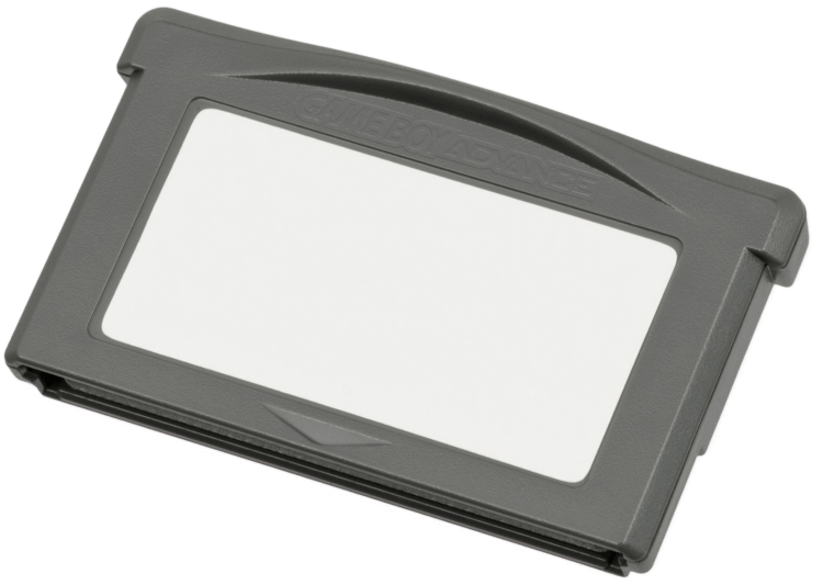
Games are distributed in a new proprietary cartridge format; it’s still called Game Pak but features a smaller design.
Programming for the GBA shares some philosophies with the Super Nintendo but also inherits the advancements of the early 2000s, such as standardised high-level languages, reliable compilers, debuggable RISC CPUs, non-proprietary workstations for development, comparatively better documentation and… access to the World Wide Web!
That said, GBA programs are mostly written in C, with performance-critical sections in assembly (ARM and Thumb) to save cycles. The official SDK that Nintendo supplied to authorised game studios contained libraries and compilers.
Accessing cartridge data
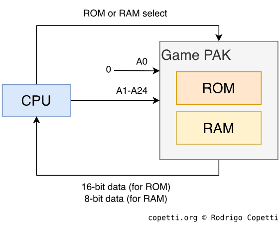
While the ARM7 has a 32-bit address bus, there are only 24 address lines connected to the cartridge.
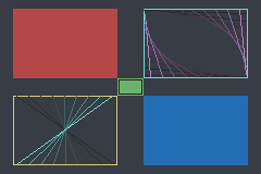
This means that, in theory, up to 16 MB can be accessed on the cartridge without needing a mapper. However, if we take a look at the memory map, it shows that 32 MB of cartridge ROM are accessible[40]. So, what’s happening here? The truth is, the Game Pak employs 25-bit addresses (which explains that 32 MB block), but its least significant bit is fixed at zero. Thus, only the remaining 24 bits are set. That’s how Game Pak addressing works.
Representation of the Game Pak addressing model. Notice how the last bit of the 25-bit address (named ‘A0’) is always zero. I must also point out that, in reality, the address and data pins are also shared/multiplexed.
Now, does this mean that data located at odd addresses (with the least significant bit at 1) is inaccessible? No, because the data bus is 16-bit: For each transfer, the CPU or DMA fetches the addressed byte plus the next, enabling to read both even and odd addresses. As you can see, this is just another work of engineering that makes full use of hardware capabilities while reducing costs.
Curiously enough, earlier 26-bit ARM CPUs also resorted to the same technique. These housed a 24-bit Program Counter, as the bits had to be multiples of eight (a.k.a. word aligned), meaning the last two bits of the 26-bit address were always zero. However, since these CPUs fetch 32 bits (the addressed byte plus the next three), the entire 26-bit address space can still be accessed.
Cartridge RAM space
To hold saves, Game Paks could either include [41]:
Static RAM (SRAM): This is volatile storage, so it needs a battery to retain its content. The console’s wiring makes SRAM accessible through the CPU’s memory map, where it can size up to 64 KB (although commercial games did not exceed 32 KB).
Flash ROM: Similar to SRAM but without the need for a battery. However, it has a limited number of write cycles.
Electrically Erasable Programmable ROM (EEPROM): These require a serial interface and can theoretically scale to any size (often found up to 8 KB).
Accessories
Throughout its lifespan, the GBA enjoyed an interesting range of accessories that reimagined how this console could be used. Many of the peripherals devised took advantage of Multiboot, the versatility of the EXT port, and the flexibility of the Game Pak slot.
Speaking of which, the earlier Game Boy Link connection (also called ‘EXT’ or serial interface) got an update again. The same 6 pins that brought multiplayer capabilities and accessories persisted, but the electronics behind each pin evolved significantly.
First things first, the new Link cable that was designed for the GBA exhibits a few new traits:
Distinct colouring and sizing: One end is purple, while the other is grey and larger. Behind the scenes lies a hardwired hierarchy: the purple end designates the connected console as the master, and the gray end designates the slave.
An extra socket in the middle of the cable: This enables daisy-chaining another GBA Link cable using the purple/master plug.
The new design makes it incompatible with the previous consoles (and games). However, it can now easily chain up to four GBAs, thereby standardising larger multiplayer arenas.
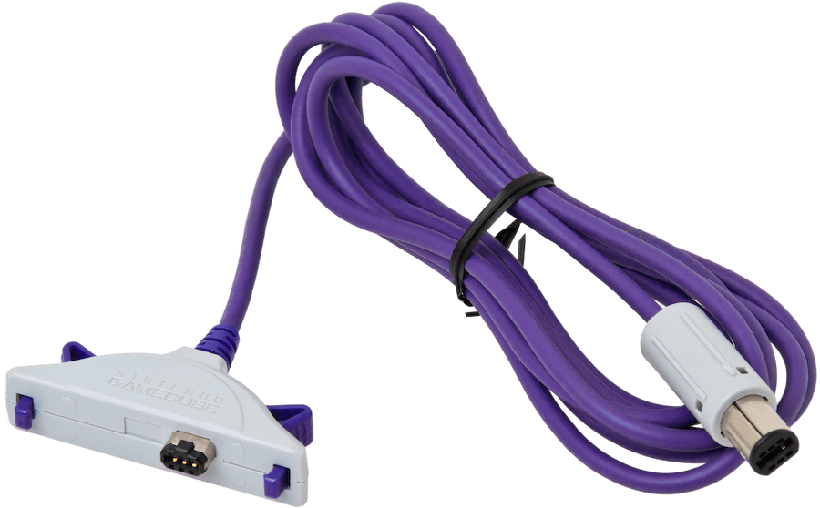
Additionally, Nintendo also shipped a variant of the GBA Link cable called the ‘GameCube-Game Boy Advance Link cable’, which is specifically wired to connect a GBA to a GameCube, I explain more later.
From the console side, the original serial connection was expanded with extra modes of operation, selected with the use of two registers.
These modes are grouped into two categories:
Synchronous modes, based on the Serial Peripheral Interface (SPI) protocol. This protocol reserves one pin to drive the clock, which the master (denoted by the purple plug) uses to set the pace.
This is how the Link connection of the Game Boy and Game Boy Color always operate.
Asynchronous modes, based on the Universal Asynchronous Receiver-Transmitter (UART) interface. There’s no clock directing the signal; the only arrangement is a common baud rate (number of bits per second) defined by the game. The master console simply signals the start and end of each transfer.
Removing the need for a clock frees lines that are used instead to coordinate the transfer between each console.
GBA games can choose between synchronous and asynchronous modes, while Game Boy titles running on the GBA are restricted to their legacy SPI modes. ‘Officially’, the latter only support the original Link cable, but here’s the interesting part: GB games also work with two GBA Link cables daisy-chained and connected to the consoles through the gray endpoints (making the two consoles slaves). This is because that arrangement cross-wires the data lines between the two consoles, replicating the setup of the original Link cable.
The EXT connector provides four programmable pins, which the console manages through these modes of operation [42]:
Normal Mode, using the SPI protocol. It’s primarily designed to exchange data between a GBA and an accessory. The interface can send and receive packets of 8 or 32 bits, and operates at either 256 KHz or 2 MHz, achieving transfers of 32 KB/s or 250 KB/s, respectively. This is quite fast, however, due to reliability issues, the faster speed is only intended for accessories directly connected to the socket (without a cable).
Even though the speed is high, it’s up to the ARM CPU (running at 16.78 MHz) to digest the transferred data in time, which may be a challenge given that it’s busy with many other tasks.
Multi-player Mode, using UART. In exchange for speed, it enables to communicate with up to four daisy-chained GBAs. Essentially, the four GBAs take turns broadcasting a 16-bit packet over the same data line. To make this work, each GBA signals the next one to transfer its packet, which is possible thanks to the wiring of the new Link cable. At the end of the transfer, all GBAs contain the packets each has sent, stored in four different 16-bit registers.
That said, remember Multiboot? This function is compatible with both Normal and Multiplayer modes. It’s up to the master to choose which. The choice depends on the number of peripherals and speed needed.
The GameCube-Game Boy Advance link cable [43], specifically crafted to connect to the GameCube’s controller port (handled by the Serial interface).
For very particular accessories, there are additional communication modes available:
UART Mode. It behaves like an RS-232 interface. Specifically, a 5-wire null modem with RTS/CTS flow control. Apart from that, it sends and receive data in 8-bit packets; and uses a FIFO buffer to queue up to four packets while they are being sent or received.
JOY BUS Mode. This is a proprietary protocol in which the GBA becomes a peripheral for the GameCube. The GBA can only receive packets, process the contents, and reply.
This is exclusively used with the ‘GameCube-Game Boy Advance Link cable’, which assigns the GBA as a slave.
General-purpose Mode. As the name indicates, all four pins become controllable by the program, enabling to implement a custom protocol.
In general terms, the use of proprietary cartridges was a major barrier compared to the constant cat-and-mouse game that other console manufacturers had to battle while using the CD-ROM medium.
To protect against bootleg cartridges (unauthorised reproductions), the GBA’s BIOS incorporated the same boot checks as those found in the original Game Boy.
Flashcarts
As solid-state storage became more affordable, a new type of cartridge appeared on the market. Flashcarts looked like ordinary Game Paks but had the addition of a re-writable memory or a card slot. This enabled users to play game ROM files within the console. The concept is not new, actually; developers have long used similar tools internally to test their games on real hardware, with manufacturers providing the equipment to enable this.
Earlier solutions included burnable NOR Flash memory (up to 32 MB) and some battery-backed SRAM. To upload binaries to the Flashcart cartridge, the box bundled a Link-to-USB cable for use with a GBA and a PC running Windows XP. With the use of proprietary flasher software and drivers, the computer uploaded a Multiboot program to the GBA, which in turn transferred a game binary from the PC to the Flashcart (inserted in the GBA). Overall, the whole task was deemed too sluggish. So, later Flashcarts (like the ‘EZ-Flash’) offered larger storage and could be programmed without requiring the GBA as an intermediate [44]. Finally, later revisions migrated to removable storage (SD, MiniSD, MicroSD, and whatnot).
Commercial availability of these cards proved to be a grey legal area: Nintendo condemned their use for enabling piracy, whereas some users argued that it was the only method for running Homebrew (programs developed outside game studios and consequently without the approval of Nintendo). The company’s argument was supported by the fact that flashers like the EZ-Writer assisted users in patching commercial ROMs, so they could run on EZ-Flash carts without issues. Following Nintendo’s legal action, these cartridges were banned in some countries (such as the UK). Nonetheless, they persisted worldwide.
That’s all folks
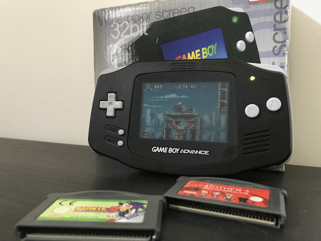
My GBA and a couple of games. Too bad it doesn’t have a backlight!
Contributing
This article is part of the Architecture of Consoles series. If you found it interesting then please consider donating. Your contribution will be used to fund the purchase of tools and resources that will help me to improve the quality of existing articles and upcoming ones.
You can also buy the book editions in English. I treat profits as donations.
A list of desirable tools and latest acquisitions for this article are tracked in here:
### Interesting hardware to get (ordered by priority)

- Any Dev kit (only if found at a reasonable price)

### Acquired tools used

- Original GBA (£40)
- The two games analysed in the article (£20)
This work is licensed under a Creative Commons Attribution 4.0 International License. You may use it for your work at no cost, even for commercial purposes. But you have to respect the license and reference the article properly. Please take a look at the following guidelines and permissions:
Article information and referencing
For any referencing style, you can use the following information:
Title of article: Game Boy Advance Architecture - A Practical Analysis
@misc{copetti-gba,url={https://www.copetti.org/writings/consoles/game-boy-advance/},title={Game Boy Advance Architecture - A Practical Analysis},author={Rodrigo Copetti},year={2019}}
or a IEEE style citation:
[1]R. Copetti, "Game Boy Advance Architecture - A Practical Analysis", Copetti.org, 2019. [Online]. Available: https://www.copetti.org/writings/consoles/game-boy-advance/. [Accessed: day- month- year].
Special use in multimedia (Youtube, Twitch, etc)
I only ask that you at least state the author’s name, the title of the article and the URL of the article, using any style of choice.
You don’t have to include all the information in the same place if it’s not feasible. For instance, if you use the article’s imagery in a Youtube video, you may state either the author’s name or URL of the article at the bottom of the image, and then include the complete reference in the video description. In other words, for any resource used from this website, let your viewers know where it originates from.
This is a very nice example because the channel shows this website directly and their viewers know where to find it. In fact, I was so impressed with their content and commentary that I gave them an interview 🙂.
Appreciated additions
If this article has significantly contributed to your work, I would appreciate it if you could dedicate an acknowledgement section, just like I do with the people and communities that helped me.
This is of course optional and beyond the requirements of the CC license, but I think it’s a nice detail that makes us, the random authors on the net, feel part of something bigger.
Third-party publishing
If you are interested in publishing this article on a third-party website, please get in touch.
If you have translated an article and wish to publish it on a third-party website, I tend to be open about it, but please contact me first.
It’s always nice to keep a record of changes. For a complete report, you can check the commit log. Alternatively, here’s a simplified list:
### 2025-12-01
- Overall improvements to prepare for a book release.
- Improved information on GB compatibility. See https://github.com/flipacholas/Architecture-of-consoles/issues/396 (thanks @Dwedit).
- Added information about hidden PPU modes. See https://github.com/flipacholas/Architecture-of-consoles/issues/397 (thanks @Sono and members of Gbadev).
- Improved sprite information. See https://github.com/flipacholas/Architecture-of-consoles/issues/425 (thanks @Kirby0Louise)
### 2024-01-05
- Extended CPU section with lots of history and descriptions of the ARM7TDMI. Thanks for the book, @dpt.
### 2021-05-18
- Renamed Gameboy CPU from 'LR35902' to 'SM83' (see Gameboy article's changelog for reason).
### 2021-03-03
- Added 'Operating System' section with BIOS breakdown.
### 2021-01-06
- Added memory diagram.
- Big set of corrections and additions (see https://github.com/flipacholas/Architecture-of-consoles/issues/20), thanks @Dwedit, @selb and @AntonioND.
- Improved 'Sources' format.
### 2020-09-19
- Corrected grammar and added content, thanks @dpt- Expanded section about gamepak's 25-bit addressing
### 2020-08-22
- Clarified tile section
### 2019-12-09
- Even better Thumb explanation.
- Added more audio info.
### 2019-10-03
- Improved Thumb explanation
### 2019-09-17
- Added a quick introduction
### 2019-09-01
- Added my GBA 🧐
### 2019-08-26
- Used better wording on some explanations
### 2019-08-19
- Corrected wee mistakes
### 2019-08-18
- Ready for publication
Rodrigo Copetti
I hope you have enjoyed this article! If you want to know more about the author tap here and if you would like to support him tap here instead


